 |
データシートサーチシステム |
|
|
データシートサーチシステム |
|
The question interval is too short.
Please try again in a few seconds.

Hello, Please ask a question about APT60M75L2LL Datasheet
# Example questions:
➢ What happens to the device's safe operating limits as drain current increases?
➢ How does increasing the drain current generally affect the switching energy (eon and eoff)?
➢ Examine figure 17 (switching energy vs. gate resistance). what is the general relationship between gate resistance and switching energy?
| Part No. | APT60M75L2LL |
| Manufacturer | ADPOW |
| Size | 155 Kbytes |
| Pages | 5 pages |
| Description | POWER MOS 7 R MOSFET |


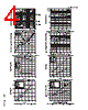


1. General Information
️· Part Number: APT60M75L2LL
️· Type: Power MOSFET (N-Channel)
️· Package: (Not explicitly stated but appears to be surface mount - likely D2PAK or similar based on the graphics)
️· Applications: Likely intended for high-power switching applications.
️· EON Includes: The datasheet mentions EON which includes diode reverse recovery.
2. Electrical Characteristics (Key Values - These are approximate from the document and subject to variation with test conditions)
️· V<sub>DS</sub> (Drain-Source Voltage): 75V (Maximum)
️· V<sub>GS</sub> (Gate-Source Voltage): ±20V (Maximum)
️· I<sub>D</sub> (Continuous Drain Current): 73A (at 25°C - this will be lower at higher temperatures)
️· R<sub>DS(on)</sub> (Drain-Source On-Resistance): (This varies significantly based on gate voltage.)
- V<sub>GS</sub> = 10V: (Value not directly given but inferred to be relatively low)
- V<sub>GS</sub> = 20V: 29 mΩ (approximate, from Figure 12)
️· V<sub>SD</sub> (Source-Drain Diode Forward Voltage): < 1.2V (at I<sub>SD</sub> = 73A)
️· Threshhold voltage: Values are given in graphs.
3. Thermal Characteristics
️· (Not explicitly listed in a table but crucial for MOSFET operation). This datasheet heavily implies a need to manage power dissipation. You're highly encouraged to consult the packaging manufacturers documentation to determine the appropriate heat sink requirements for safe operation.
4. Dynamic/Switching Characteristics (Very important for high-frequency applications)
️· Switching Times: Shown in Figure 14 and 15 (Delay Times, Rise and Fall Times). These values are dependent on load conditions (Inductance – L) and gate resistance (R<sub>G</sub>).
️· Switching Energy: Shown in Figure 16 and 17. The switching energy is directly affected by both inductance and gate resistance.
️· Capacitances: Figure 11 shows capacitance versus drain-source voltage:
- C<sub>iss</sub> (Input Capacitance)
- C<sub>oss</sub> (Output Capacitance)
- C<sub>rss</sub> (Reverse Transfer Capacitance)
5. Important Graphs and Figures (Brief Descriptions)
️· Figure 12: R<sub>DS(on)</sub> vs. Gate-Source Voltage: Shows how on-resistance decreases as gate voltage increases.
️· Figure 13: Source-Drain Diode Forward Voltage vs. Current: Shows the forward voltage drop across the body diode.
️· Figure 14 & 15: Delay Times vs. Current & Rise/Fall Times vs. Current: Shows how switching times are influenced by current and load inductance.
️· Figure 16 & 17: Switching Energy vs. Current & Gate Resistance: Highlights the impact of load inductance and gate resistance on switching losses.
️· Figure 11: Capacitances vs. Drain-Source Voltage: Important for high frequency application design.
6. Operational Considerations & Key Takeaways
️· Gate Resistance (R<sub>G</sub>): The gate resistance has a significant impact on switching performance. Lower gate resistance generally leads to faster switching but higher gate charge. There’s a trade-off.
️· Inductance (L): Parasitic inductance in the circuit dramatically affects switching times and energy losses. Minimize inductance.
️· Thermal Management: This is a high-power device. Adequate heat sinking is *essential* to prevent overheating and ensure reliable operation. Consult the package manufacturer's datasheet for thermal resistance values.
️· Body Diode: The MOSFET has an internal body diode which is important for freewheeling applications.
1. General Information
️· Part Number: APT60M75L2LL
️· Type: Power MOSFET (N-Channel)
️· Package: (Not explicitly stated but appears to be surface mount - likely D2PAK or similar based on the graphics)
️· Applications: Likely intended for high-power switching applications.
️· EON Includes: The datasheet mentions EON which includes diode reverse recovery.
2. Electrical Characteristics (Key Values - These are approximate from the document and subject to variation with test conditions)
️· V<sub>DS</sub> (Drain-Source Voltage): 75V (Maximum)
️· V<sub>GS</sub> (Gate-Source Voltage): ±20V (Maximum)
️· I<sub>D</sub> (Continuous Drain Current): 73A (at 25°C - this will be lower at higher temperatures)
️· R<sub>DS(on)</sub> (Drain-Source On-Resistance): (This varies significantly based on gate voltage.)
- V<sub>GS</sub> = 10V: (Value not directly given but inferred to be relatively low)
- V<sub>GS</sub> = 20V: 29 mΩ (approximate, from Figure 12)
️· V<sub>SD</sub> (Source-Drain Diode Forward Voltage): < 1.2V (at I<sub>SD</sub> = 73A)
️· Threshhold voltage: Values are given in graphs.
3. Thermal Characteristics
️· (Not explicitly listed in a table but crucial for MOSFET operation). This datasheet heavily implies a need to manage power dissipation. You're highly encouraged to consult the packaging manufacturers documentation to determine the appropriate heat sink requirements for safe operation.
4. Dynamic/Switching Characteristics (Very important for high-frequency applications)
️· Switching Times: Shown in Figure 14 and 15 (Delay Times, Rise and Fall Times). These values are dependent on load conditions (Inductance – L) and gate resistance (R<sub>G</sub>).
️· Switching Energy: Shown in Figure 16 and 17. The switching energy is directly affected by both inductance and gate resistance.
️· Capacitances: Figure 11 shows capacitance versus drain-source voltage:
- C<sub>iss</sub> (Input Capacitance)
- C<sub>oss</sub> (Output Capacitance)
- C<sub>rss</sub> (Reverse Transfer Capacitance)
5. Important Graphs and Figures (Brief Descriptions)
️· Figure 12: R<sub>DS(on)</sub> vs. Gate-Source Voltage: Shows how on-resistance decreases as gate voltage increases.
️· Figure 13: Source-Drain Diode Forward Voltage vs. Current: Shows the forward voltage drop across the body diode.
️· Figure 14 & 15: Delay Times vs. Current & Rise/Fall Times vs. Current: Shows how switching times are influenced by current and load inductance.
️· Figure 16 & 17: Switching Energy vs. Current & Gate Resistance: Highlights the impact of load inductance and gate resistance on switching losses.
️· Figure 11: Capacitances vs. Drain-Source Voltage: Important for high frequency application design.
6. Operational Considerations & Key Takeaways
️· Gate Resistance (R<sub>G</sub>): The gate resistance has a significant impact on switching performance. Lower gate resistance generally leads to faster switching but higher gate charge. There’s a trade-off.
️· Inductance (L): Parasitic inductance in the circuit dramatically affects switching times and energy losses. Minimize inductance.
️· Thermal Management: This is a high-power device. Adequate heat sinking is *essential* to prevent overheating and ensure reliable operation. Consult the package manufacturer's datasheet for thermal resistance values.
️· Body Diode: The MOSFET has an internal body diode which is important for freewheeling applications.
| Part No. | APT60M75L2LL |
| Manufacturer | ADPOW |
| Size | 155 Kbytes |
| Pages | 5 pages |
| Description | POWER MOS 7 R MOSFET |
| ALLDATASHEETはお客様のビジネスに役立ちますか? [ DONATE ] |
Alldatasheetは | 広告 | お問い合わせ | プライバシーポリシー | データシートへのリンク | リンク交換 | メーカーリスト All Rights Reserved©Alldatasheet.com |
| Russian : Alldatasheetru.com | Korean : Alldatasheet.co.kr | Spanish : Alldatasheet.es | French : Alldatasheet.fr | Italian : Alldatasheetit.com Portuguese : Alldatasheetpt.com | Polish : Alldatasheet.pl | Vietnamese : Alldatasheet.vn Indian : Alldatasheet.in | Mexican : Alldatasheet.com.mx | British : Alldatasheet.co.uk | New Zealand : Alldatasheet.co.nz |
|
Family Site : ic2ic.com |
icmetro.com |
 Japanese ▼
  English
 Chinese
 German
 Russian
 Korean
 Spanish
 French
 Italian
 Portuguese
 Polish
 Vietnamese
 Indian
 Mexican
 British
 New Zealand