 |
データシートサーチシステム |
|
|
データシートサーチシステム |
|
The question interval is too short.
Please try again in a few seconds.

Hello, Please ask a question about WS27C256L Datasheet
# Example questions:
➢ What is the typical input capacitance (cin) of the device, and under what voltage condition is this value specified?
➢ What capacitor values are recommended in parallel to ensure proper device operation?
➢ What test load is used for a.c. testing, including capacitance and resistance values?
| Part No. | WS27C256L |
| Manufacturer | STMICROELECTRONICS |
| Size | 48 Kbytes |
| Pages | 5 pages |
| Description | Military 32K x 8 CMOS EPROM |


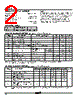


Document Focus: This excerpt details the AC and DC characteristics of a memory device (likely a static RAM or similar) designated by the model number *WS013A-16*. It provides timing parameters, capacitance values, and testing conditions.
1. Input/Output Logic Levels:
️· V<sub>IH</sub> (High-Level Input Voltage): 2.0V - 2.4V
️· V<sub>IL</sub> (Low-Level Input Voltage): 0.4V
️· V<sub>OH</sub> (High-Level Output Voltage): 2.0V
️· V<sub>OL</sub> (Low-Level Output Voltage): 0.8V
2. Key Timing Parameters (AC Characteristics): These specify how fast the device can respond. Several parameters are listed, including:
️· t<sub>OH</sub>: Output Hold Time
️· t<sub>OCX</sub>: (Information missing in the extract, but it's a timing parameter.)
️· t<sub>ACC</sub> (Not shown): Access Time. (likely found elsewhere in the datasheet)
3. Capacitance Values:
️· C<sub>IN</sub> (Input Capacitance): 4-6 pF
️· C<sub>OUT</sub> (Output Capacitance): 8-12 pF
️· C<sub>VPP</sub> (VPP Capacitance): 18-25 pF
4. Test Conditions:
️· Test Load: 100 pF (including scope and jig capacitance) in parallel with 820Ω resistor.
️· Supply Voltage: 2.01 V
️· Input Drive: 2.4V for logic '1', 0.4V for logic '0'.
️· Measurements: Made at 2.0 V for logic '1' and 0.8 V for logic '0'.
5. Important Notes:
️· Decoupling Capacitance: The datasheet *strongly* recommends using decoupling capacitors (0.1 µF in parallel with 0.01 µF) as close as possible to the device. This is crucial for achieving published performance and preventing access time degradation or transient failures.
️· Sampling: Some parameters are “only sampled and not 100% tested.”
6. Documentation Structure:
️· The excerpt presents data in tables for easy reference.
️· Multiple Columns repeat the same information.
In summary, this excerpt provides crucial timing and electrical characteristics necessary for properly interfacing with and designing systems around the memory device WS013A-16. It highlights the importance of proper power supply decoupling and adherence to specified test conditions.
Document Focus: This excerpt details the AC and DC characteristics of a memory device (likely a static RAM or similar) designated by the model number *WS013A-16*. It provides timing parameters, capacitance values, and testing conditions.
1. Input/Output Logic Levels:
️· V<sub>IH</sub> (High-Level Input Voltage): 2.0V - 2.4V
️· V<sub>IL</sub> (Low-Level Input Voltage): 0.4V
️· V<sub>OH</sub> (High-Level Output Voltage): 2.0V
️· V<sub>OL</sub> (Low-Level Output Voltage): 0.8V
2. Key Timing Parameters (AC Characteristics): These specify how fast the device can respond. Several parameters are listed, including:
️· t<sub>OH</sub>: Output Hold Time
️· t<sub>OCX</sub>: (Information missing in the extract, but it's a timing parameter.)
️· t<sub>ACC</sub> (Not shown): Access Time. (likely found elsewhere in the datasheet)
3. Capacitance Values:
️· C<sub>IN</sub> (Input Capacitance): 4-6 pF
️· C<sub>OUT</sub> (Output Capacitance): 8-12 pF
️· C<sub>VPP</sub> (VPP Capacitance): 18-25 pF
4. Test Conditions:
️· Test Load: 100 pF (including scope and jig capacitance) in parallel with 820Ω resistor.
️· Supply Voltage: 2.01 V
️· Input Drive: 2.4V for logic '1', 0.4V for logic '0'.
️· Measurements: Made at 2.0 V for logic '1' and 0.8 V for logic '0'.
5. Important Notes:
️· Decoupling Capacitance: The datasheet *strongly* recommends using decoupling capacitors (0.1 µF in parallel with 0.01 µF) as close as possible to the device. This is crucial for achieving published performance and preventing access time degradation or transient failures.
️· Sampling: Some parameters are “only sampled and not 100% tested.”
6. Documentation Structure:
️· The excerpt presents data in tables for easy reference.
️· Multiple Columns repeat the same information.
In summary, this excerpt provides crucial timing and electrical characteristics necessary for properly interfacing with and designing systems around the memory device WS013A-16. It highlights the importance of proper power supply decoupling and adherence to specified test conditions.
| Part No. | WS27C256L |
| Manufacturer | STMICROELECTRONICS |
| Size | 48 Kbytes |
| Pages | 5 pages |
| Description | Military 32K x 8 CMOS EPROM |
| ALLDATASHEETはお客様のビジネスに役立ちますか? [ DONATE ] |
Alldatasheetは | 広告 | お問い合わせ | プライバシーポリシー | データシートへのリンク | リンク交換 | メーカーリスト All Rights Reserved©Alldatasheet.com |
| Russian : Alldatasheetru.com | Korean : Alldatasheet.co.kr | Spanish : Alldatasheet.es | French : Alldatasheet.fr | Italian : Alldatasheetit.com Portuguese : Alldatasheetpt.com | Polish : Alldatasheet.pl | Vietnamese : Alldatasheet.vn Indian : Alldatasheet.in | Mexican : Alldatasheet.com.mx | British : Alldatasheet.co.uk | New Zealand : Alldatasheet.co.nz |
|
Family Site : ic2ic.com |
icmetro.com |
 Japanese ▼
  English
 Chinese
 German
 Russian
 Korean
 Spanish
 French
 Italian
 Portuguese
 Polish
 Vietnamese
 Indian
 Mexican
 British
 New Zealand