 |
データシートサーチシステム |
|
|
データシートサーチシステム |
|
The question interval is too short.
Please try again in a few seconds.
| Part No. | X24C04 |
| Manufacturer | XICOR |
| Size | 78 Kbytes |
| Pages | 18 pages |
| Description | Serial E2PROM |





1. General Description:
️· The X24C04 is a 256x8 (2048) EEPROM (Electrically Erasable Programmable Read-Only Memory) organized as 256 pages of 8 bytes each.
️· It's designed for I²C compatible serial interfaces.
️· It's non-volatile, meaning it retains data when power is removed.
️· It is suitable for data storage applications.
2. Electrical Characteristics (Key Parameters):
️· Supply Voltage (Vcc): Not explicitly given in this excerpt, but it's assumed to be a standard EEPROM voltage range.
️· Input Voltage Range (Vih/Vil): Vih is the minimum high-level input voltage; Vil is the maximum low-level input voltage. The documentation mentions V x 0.1 to V x 0.9 for input pulse levels, so 0.1 to 0.9*Vcc would be the range. Specific values are not given.
️· Operating Temperature Range: Not given in the provided text.
️· Data Retention: Not given in the provided text.
️· Write/Erase Cycle Endurance: Not given in the provided text.
3. I²C Interface Details:
️· Address: The I²C slave address is not mentioned. This is crucial for communication.
️· Clock Speed (fSCL): Maximum clock frequency is 100 kHz.
️· Start/Stop Conditions:
- Start Condition Hold Time (tHD:STA): 4.0 µs
- Stop Condition Setup Time (tSU:STO): 4.7 µs
️· Data Timing:
- Data In Setup Time (tSU:DAT): 250 ns
- Data In Hold Time (tDH): 300 ns
- Time from SCL Low to SDA Data Out Valid (tAA): 3.5 µs
️· Bus Free Time: 4.7 µs before a new transmission can start (tBUF).
️· Rise/Fall Times: Maximum 1 µs rise and 300 ns fall times for SDA and SCL signals.
️· Power-up Timing
* Time from power up to read operation (tPUR): 1 ms
* Time from power up to write operation (tPUW): 5 ms
4. A.C. Conditions of Test
️· Input Pulse Levels: V x 0.1 to V x 0.9 (where V is the supply voltage)
️· Input Rise/Fall Times: 10 ns.
Important Notes and Missing Information:
️· Slave Address: The I²C slave address is *not* provided in this excerpt. This is essential for communication. Without it, you cannot address the EEPROM.
️· Write Protection: Details regarding write protection (if any) are missing.
️· Operating Voltages and Ranges: Specific voltage values are not included.
️· Detailed Command Sequences: The documentation does not provide sequences for read, write, and erase operations.
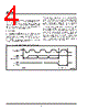
️· Timing Diagrams: There are numerous timing diagrams included, which graphically show the relationships between signals (SDA, SCL, etc.). These are critical for understanding the timing requirements.
Where to Find More Information:
1. General Description:
️· The X24C04 is a 256x8 (2048) EEPROM (Electrically Erasable Programmable Read-Only Memory) organized as 256 pages of 8 bytes each.
️· It's designed for I²C compatible serial interfaces.
️· It's non-volatile, meaning it retains data when power is removed.
️· It is suitable for data storage applications.
2. Electrical Characteristics (Key Parameters):
️· Supply Voltage (Vcc): Not explicitly given in this excerpt, but it's assumed to be a standard EEPROM voltage range.
️· Input Voltage Range (Vih/Vil): Vih is the minimum high-level input voltage; Vil is the maximum low-level input voltage. The documentation mentions V x 0.1 to V x 0.9 for input pulse levels, so 0.1 to 0.9*Vcc would be the range. Specific values are not given.
️· Operating Temperature Range: Not given in the provided text.
️· Data Retention: Not given in the provided text.
️· Write/Erase Cycle Endurance: Not given in the provided text.
3. I²C Interface Details:
️· Address: The I²C slave address is not mentioned. This is crucial for communication.
️· Clock Speed (fSCL): Maximum clock frequency is 100 kHz.
️· Start/Stop Conditions:
- Start Condition Hold Time (tHD:STA): 4.0 µs
- Stop Condition Setup Time (tSU:STO): 4.7 µs
️· Data Timing:
- Data In Setup Time (tSU:DAT): 250 ns
- Data In Hold Time (tDH): 300 ns
- Time from SCL Low to SDA Data Out Valid (tAA): 3.5 µs
️· Bus Free Time: 4.7 µs before a new transmission can start (tBUF).
️· Rise/Fall Times: Maximum 1 µs rise and 300 ns fall times for SDA and SCL signals.
️· Power-up Timing
* Time from power up to read operation (tPUR): 1 ms
* Time from power up to write operation (tPUW): 5 ms
4. A.C. Conditions of Test
️· Input Pulse Levels: V x 0.1 to V x 0.9 (where V is the supply voltage)
️· Input Rise/Fall Times: 10 ns.
Important Notes and Missing Information:
️· Slave Address: The I²C slave address is *not* provided in this excerpt. This is essential for communication. Without it, you cannot address the EEPROM.
️· Write Protection: Details regarding write protection (if any) are missing.
️· Operating Voltages and Ranges: Specific voltage values are not included.
️· Detailed Command Sequences: The documentation does not provide sequences for read, write, and erase operations.
️· Timing Diagrams: There are numerous timing diagrams included, which graphically show the relationships between signals (SDA, SCL, etc.). These are critical for understanding the timing requirements.
Where to Find More Information:
| Part No. | X24C04 |
| Manufacturer | XICOR |
| Size | 78 Kbytes |
| Pages | 18 pages |
| Description | Serial E2PROM |
| ALLDATASHEETはお客様のビジネスに役立ちますか? [ DONATE ] |
Alldatasheetは | 広告 | お問い合わせ | プライバシーポリシー | データシートへのリンク | リンク交換 | メーカーリスト All Rights Reserved©Alldatasheet.com |
| Russian : Alldatasheetru.com | Korean : Alldatasheet.co.kr | Spanish : Alldatasheet.es | French : Alldatasheet.fr | Italian : Alldatasheetit.com Portuguese : Alldatasheetpt.com | Polish : Alldatasheet.pl | Vietnamese : Alldatasheet.vn Indian : Alldatasheet.in | Mexican : Alldatasheet.com.mx | British : Alldatasheet.co.uk | New Zealand : Alldatasheet.co.nz |
|
Family Site : ic2ic.com |
icmetro.com |
 Japanese ▼
  English
 Chinese
 German
 Russian
 Korean
 Spanish
 French
 Italian
 Portuguese
 Polish
 Vietnamese
 Indian
 Mexican
 British
 New Zealand