 |
データシートサーチシステム |
|
|
データシートサーチシステム |
|
The question interval is too short.
Please try again in a few seconds.

Hello, Please ask a question about AD7674AST Datasheet
# Example questions:
➢ What is the allowable range for the analog input voltages (in+, in-, ref, refbufin, refgnd) relative to agnd?
➢ In serial interface modes, what are the two different maximum load capacitances (cl) specified, and under what conditions does each apply?
➢ What is the maximum junction temperature specified for the ad7674?
| Part No. | AD7674AST |
| Manufacturer | AD |
| Size | 983 Kbytes |
| Pages | 28 pages |
| Description | 18-Bit, 2.5 LSB INL, 800 kSPS SAR ADC |


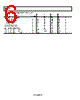
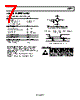
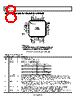
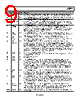




1. Device Overview
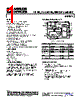
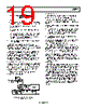
️· The AD7674 is an analog-to-digital converter (ADC).
️· It's a high-performance, low-power device likely intended for precision data acquisition.
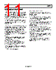
2. Absolute Maximum Ratings
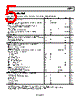
️· These are the limits beyond which the device *could* be damaged. Don't operate within these ranges!
- Analog Input Voltages: -0.3V to +7V relative to the analog ground (AGND).
- Ground Voltage Differences: Limited voltage differences between the analog, digital, and output grounds.
- Supply Voltages: Limited voltage ranges for AVDD, DVDD, and OVDD, and limits on the voltage differences between them.
- Digital Input Voltages: -0.3V to +7V
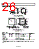
- Power Dissipation: Important thermal limits, especially if using the LQFP or LFCSP package. Overheating can damage the device.
- Temperature: Operating and storage temperature ranges.
- Lead Temperature: Limit for soldering.
️· ESD Caution: Electrostatic discharge (ESD) can damage the device. Handle with appropriate precautions.
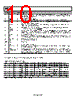
3. Timing Characteristics
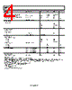
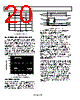
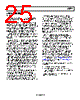
️· Serial Interface Modes: Loads on the SDOUT, SYNC, and SCLK lines must be considered. Standard is 10pF, otherwise 60pF.
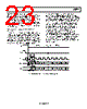
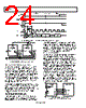
️· Multiple Timing Parameters: The datasheet provides numerous timing parameters for serial communication, including:
- SYNC setup and hold times
- SCLK period and pulse widths
- SDOUT delay and setup/hold times
- Busy signal timing.
️· Serial Clock Timings (Table 4): Specific values for serial clock timing depend on the DIVSCLK[1:0] setting. These values specify minimums and maximums for timing parameters.
4. Key Tables:
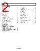
️· Table 6 (Summary): (Not provided, but implied to be present in the complete datasheet) Likely lists key features and specifications.
️· Table 5 (Absolute Maximum Ratings): As described above.
️· Table 3 (Timing Characteristics): Detailed timing information for serial interface modes.
️· Table 4 (Serial Clock Timings): Specific values for serial clock timing based on a setting.
Important Notes & What's Missing
️· This is an *excerpt*: The complete datasheet would contain far more information, including:
- ADC Resolution and Sample Rate
- Analog Input Ranges
- Power Supply Requirements
- Detailed descriptions of various modes of operation
- Application Circuits
️· Read the full datasheet! This excerpt provides a glimpse, but you need the complete document for proper design and operation.
️· Understanding the Mode: The timing characteristics are heavily dependent on the chosen operating mode (e.g., Warp, Normal, Impulse).
1. Device Overview
️· The AD7674 is an analog-to-digital converter (ADC).
️· It's a high-performance, low-power device likely intended for precision data acquisition.
2. Absolute Maximum Ratings
️· These are the limits beyond which the device *could* be damaged. Don't operate within these ranges!
- Analog Input Voltages: -0.3V to +7V relative to the analog ground (AGND).
- Ground Voltage Differences: Limited voltage differences between the analog, digital, and output grounds.
- Supply Voltages: Limited voltage ranges for AVDD, DVDD, and OVDD, and limits on the voltage differences between them.
- Digital Input Voltages: -0.3V to +7V
- Power Dissipation: Important thermal limits, especially if using the LQFP or LFCSP package. Overheating can damage the device.
- Temperature: Operating and storage temperature ranges.
- Lead Temperature: Limit for soldering.
️· ESD Caution: Electrostatic discharge (ESD) can damage the device. Handle with appropriate precautions.
3. Timing Characteristics
️· Serial Interface Modes: Loads on the SDOUT, SYNC, and SCLK lines must be considered. Standard is 10pF, otherwise 60pF.
️· Multiple Timing Parameters: The datasheet provides numerous timing parameters for serial communication, including:
- SYNC setup and hold times
- SCLK period and pulse widths
- SDOUT delay and setup/hold times
- Busy signal timing.
️· Serial Clock Timings (Table 4): Specific values for serial clock timing depend on the DIVSCLK[1:0] setting. These values specify minimums and maximums for timing parameters.
4. Key Tables:
️· Table 6 (Summary): (Not provided, but implied to be present in the complete datasheet) Likely lists key features and specifications.
️· Table 5 (Absolute Maximum Ratings): As described above.
️· Table 3 (Timing Characteristics): Detailed timing information for serial interface modes.
️· Table 4 (Serial Clock Timings): Specific values for serial clock timing based on a setting.
Important Notes & What's Missing
️· This is an *excerpt*: The complete datasheet would contain far more information, including:
- ADC Resolution and Sample Rate
- Analog Input Ranges
- Power Supply Requirements
- Detailed descriptions of various modes of operation
- Application Circuits
️· Read the full datasheet! This excerpt provides a glimpse, but you need the complete document for proper design and operation.
️· Understanding the Mode: The timing characteristics are heavily dependent on the chosen operating mode (e.g., Warp, Normal, Impulse).
| Part No. | AD7674AST |
| Manufacturer | AD |
| Size | 983 Kbytes |
| Pages | 28 pages |
| Description | 18-Bit, 2.5 LSB INL, 800 kSPS SAR ADC |
| ALLDATASHEETはお客様のビジネスに役立ちますか? [ DONATE ] |
Alldatasheetは | 広告 | お問い合わせ | プライバシーポリシー | データシートへのリンク | リンク交換 | メーカーリスト All Rights Reserved©Alldatasheet.com |
| Russian : Alldatasheetru.com | Korean : Alldatasheet.co.kr | Spanish : Alldatasheet.es | French : Alldatasheet.fr | Italian : Alldatasheetit.com Portuguese : Alldatasheetpt.com | Polish : Alldatasheet.pl | Vietnamese : Alldatasheet.vn Indian : Alldatasheet.in | Mexican : Alldatasheet.com.mx | British : Alldatasheet.co.uk | New Zealand : Alldatasheet.co.nz |
|
Family Site : ic2ic.com |
icmetro.com |
 Japanese ▼
  English
 Chinese
 German
 Russian
 Korean
 Spanish
 French
 Italian
 Portuguese
 Polish
 Vietnamese
 Indian
 Mexican
 British
 New Zealand