 |
データシートサーチシステム |
|
|
データシートサーチシステム |
|
The question interval is too short.
Please try again in a few seconds.

Hello, Please ask a question about LT1370 Datasheet
# Example questions:
➢ What is the typical switching frequency of the lt1370, and how does it vary across different temperature grades?
➢ What is the minimum input voltage required for the lt1370 to operate, and what is the typical supply current at that voltage?
➢ Describe the function of the s/s pin and its impact on the lt1370's operation, including typical current draw and threshold voltages.
| Part No. | LT1370 |
| Manufacturer | LINER |
| Size | 179 Kbytes |
| Pages | 16 pages |
| Description | 500kHz High Efficiency 6A Switching Regulator |


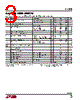



1. General Information / Operating Conditions
️· Device: LT1370 (likely with variations like LT1370HVC and LT1370HVI, I-Grade)
️· Input Voltage Range (VIN): 2.4V to 25V (minimum input voltage: 2.4V)
️· Operating Temperature Range: -40°C to 125°C (depending on grade).
️· Reference Voltage (VREF): 1.230V to 1.260V (standard), 1.225V to 1.265V (other variations). This is a crucial reference for the feedback loop.
2. Key Functional Parameters
️· Switching Frequency (f): 440 kHz to 580 kHz (varies with temperature and grade).
️· Maximum Duty Cycle: 85% (can vary to 95% depending on parameter)
️· Switch ON Resistance (VSAT): 0.065 Ω to 0.11 Ω. Lower is better for efficiency.
️· Switch Current Limit (ILIM): 6A to 10A. The current limit is dynamic and dependent on duty cycle, as detailed by the formula `ILIM = 2.65(2.7 – DC)`.
️· Shutdown Threshold: 0.6V to 2V. Determines the voltage at which the regulator shuts down.
️· Synchronization Frequency Range: 600 kHz to 800 kHz.
3. Feedback and Error Amplification
️· Error Amplifier Transconductance (gm): 700 µS to 2300 µS (This defines how effectively the error amplifier responds to feedback signal changes).
️· Error Amplifier Clamp Voltage: 0.2V to 2.3V (These limits how the error amplifier shapes the output voltage).
️· VC Pin Threshold: 0.9V to 1.35V (Voltage required on the control voltage pin to trigger switching).
4. Efficiency and Current Consumption
️· Supply Current (IQ): 4.5 mA to 6mA (This is the quiescent current when the regulator is in normal operation).
️· Shutdown Supply Current: 12 µA to 40 µA (Current when the regulator is in shutdown mode).
️· Supply Current Increase During Switch ON Time (∆IIN, ∆ISW): 22mA to 33mA (Important for transient response).
5. Other Notable Parameters
️· Shutdown Delay: 4 µs to 25 µs (Time it takes for the regulator to enter/exit shutdown).
️· S/S Input Current: -7 µA to 10 µA (Current flowing into the synchronization pin).
️· Output Switch Breakdown Voltage (BV): 35V to 47V.
Summary Table (Important Values)
| Parameter | Range | Units |
|---|---|---|
| Input Voltage (VIN) | 2.4 - 25 | V |
| VREF | 1.230 - 1.260 | V |
| Switching Frequency (f) | 440 - 580 | kHz |
| Duty Cycle (DC) | 0 - 85% (varies) | % |
| ILIM | 6 - 10 | A |
| IQ | 4.5 - 6 | mA |
1. General Information / Operating Conditions
️· Device: LT1370 (likely with variations like LT1370HVC and LT1370HVI, I-Grade)
️· Input Voltage Range (VIN): 2.4V to 25V (minimum input voltage: 2.4V)
️· Operating Temperature Range: -40°C to 125°C (depending on grade).
️· Reference Voltage (VREF): 1.230V to 1.260V (standard), 1.225V to 1.265V (other variations). This is a crucial reference for the feedback loop.
2. Key Functional Parameters
️· Switching Frequency (f): 440 kHz to 580 kHz (varies with temperature and grade).
️· Maximum Duty Cycle: 85% (can vary to 95% depending on parameter)
️· Switch ON Resistance (VSAT): 0.065 Ω to 0.11 Ω. Lower is better for efficiency.
️· Switch Current Limit (ILIM): 6A to 10A. The current limit is dynamic and dependent on duty cycle, as detailed by the formula `ILIM = 2.65(2.7 – DC)`.
️· Shutdown Threshold: 0.6V to 2V. Determines the voltage at which the regulator shuts down.
️· Synchronization Frequency Range: 600 kHz to 800 kHz.
3. Feedback and Error Amplification
️· Error Amplifier Transconductance (gm): 700 µS to 2300 µS (This defines how effectively the error amplifier responds to feedback signal changes).
️· Error Amplifier Clamp Voltage: 0.2V to 2.3V (These limits how the error amplifier shapes the output voltage).
️· VC Pin Threshold: 0.9V to 1.35V (Voltage required on the control voltage pin to trigger switching).
4. Efficiency and Current Consumption
️· Supply Current (IQ): 4.5 mA to 6mA (This is the quiescent current when the regulator is in normal operation).
️· Shutdown Supply Current: 12 µA to 40 µA (Current when the regulator is in shutdown mode).
️· Supply Current Increase During Switch ON Time (∆IIN, ∆ISW): 22mA to 33mA (Important for transient response).
5. Other Notable Parameters
️· Shutdown Delay: 4 µs to 25 µs (Time it takes for the regulator to enter/exit shutdown).
️· S/S Input Current: -7 µA to 10 µA (Current flowing into the synchronization pin).
️· Output Switch Breakdown Voltage (BV): 35V to 47V.
Summary Table (Important Values)
| Parameter | Range | Units |
|---|---|---|
| Input Voltage (VIN) | 2.4 - 25 | V |
| VREF | 1.230 - 1.260 | V |
| Switching Frequency (f) | 440 - 580 | kHz |
| Duty Cycle (DC) | 0 - 85% (varies) | % |
| ILIM | 6 - 10 | A |
| IQ | 4.5 - 6 | mA |
| Part No. | LT1370 |
| Manufacturer | LINER |
| Size | 179 Kbytes |
| Pages | 16 pages |
| Description | 500kHz High Efficiency 6A Switching Regulator |
| ALLDATASHEETはお客様のビジネスに役立ちますか? [ DONATE ] |
Alldatasheetは | 広告 | お問い合わせ | プライバシーポリシー | データシートへのリンク | リンク交換 | メーカーリスト All Rights Reserved©Alldatasheet.com |
| Russian : Alldatasheetru.com | Korean : Alldatasheet.co.kr | Spanish : Alldatasheet.es | French : Alldatasheet.fr | Italian : Alldatasheetit.com Portuguese : Alldatasheetpt.com | Polish : Alldatasheet.pl | Vietnamese : Alldatasheet.vn Indian : Alldatasheet.in | Mexican : Alldatasheet.com.mx | British : Alldatasheet.co.uk | New Zealand : Alldatasheet.co.nz |
|
Family Site : ic2ic.com |
icmetro.com |
 Japanese ▼
  English
 Chinese
 German
 Russian
 Korean
 Spanish
 French
 Italian
 Portuguese
 Polish
 Vietnamese
 Indian
 Mexican
 British
 New Zealand