|
データシートサーチシステム |
|
|
データシートサーチシステム |
|
M30620FCAFP データシート(PDF) 177 Page - Mitsubishi Electric Semiconductor |
|
|
|||||||||||||||||||||||||||||
M30620FCAFP データシート(HTML) 177 Page - Mitsubishi Electric Semiconductor |
|
|
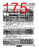
177 / 274 page  Mitsubishi microcomputers M16C / 62A Group SINGLE-CHIP 16-BIT CMOS MICROCOMPUTER Timing (Vcc = 5V) 177 Timing requirements (referenced to VCC = 5V, VSS = 0V at Topr = – 20oC to 85oC / – 40oC to 85oC (*) unless otherwise specified) * : Specify a product of -40 °C to 85°C to use it. f(BCLK) X 2 (Note) (Note) (Note) 40 30 0 0 40 0 Note: Calculated according to the BCLK frequency as follows: 40 Max. External clock rise time ns tr Min. External clock input cycle time External clock input HIGH pulse width External clock input LOW pulse width External clock fall time ns ns ns ns tc tw(H) tw(L) tf Parameter Symbol Unit Standard 15 62.5 25 25 15 Min. Data input setup time ns tsu(DB-RD) tsu(RDY-BCLK ) Parameter Symbol Unit Max. Standard ns RDY input setup time Data input hold time ns th(RD-DB) th(BCLK -RDY) ns RDY input hold time ns HOLD input setup time tsu(HOLD-BCLK ) ns HOLD input hold time th(BCLK-HOLD ) Data input access time (no wait) ns tac1(RD-DB) ns ns tac2(RD-DB) tac3(RD-DB) Data input access time (with wait) Data input access time (when accessing multiplex bus area) ns td(BCLK-HLDA ) HLDA output delay time tac1(RD – DB) = f(BCLK) X 2 – 45 10 9 [ns] tac2(RD – DB) = f(BCLK) X 2 – 45 3 X 10 9 [ns] tac3(RD – DB) = – 45 3 X 10 9 [ns] VCC = 5V Table 1.23.8. Memory expansion and microprocessor modes Table 1.23.7. External clock input |
|
リンク URL |
| ALLDATASHEETはお客様のビジネスに役立ちますか? [ DONATE ] |
Alldatasheetは | 広告 | お問い合わせ | プライバシーポリシー | データシートへのリンク | リンク交換 | メーカーリスト All Rights Reserved©Alldatasheet.com |
| Russian : Alldatasheetru.com | Korean : Alldatasheet.co.kr | Spanish : Alldatasheet.es | French : Alldatasheet.fr | Italian : Alldatasheetit.com Portuguese : Alldatasheetpt.com | Polish : Alldatasheet.pl | Vietnamese : Alldatasheet.vn Indian : Alldatasheet.in | Mexican : Alldatasheet.com.mx | British : Alldatasheet.co.uk | New Zealand : Alldatasheet.co.nz |
|
Family Site : ic2ic.com |
icmetro.com |
 Japanese ▼
 English
 Chinese
 German
 Japanese
 Russian
 Korean
 Spanish
 French
 Italian
 Portuguese
 Polish
 Vietnamese
 Indian
 Mexican
 British
 New Zealand