 |
データシートサーチシステム |
|
|
データシートサーチシステム |
|
The question interval is too short.
Please try again in a few seconds.

Hello, Please ask a question about ACT4533 Datasheet
# Example questions:
➢ The document details a method for compensating for cable resistance in a charger. explain how this compensation is achieved, and what component is adjusted to implement it.
➢ The document provides a table of suggested component values for different output voltages and capacitor types. what parameters are considered when determining these values, and why is this compensation important?
➢ List at least three crucial considerations or recommendations provided in the 'pc board layout guidance' section to ensure proper operation of the ic.
| Part No. | ACT4533 |
| Manufacturer | ACTIVE-SEMI |
| Size | 602 Kbytes |
| Pages | 16 pages |
| Description | Wide-Input Sensorless CC/CV Step-Down DC/DC Converter |




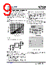

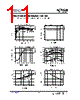




1. Overview & Purpose:
️· The document describes the ACT4533, a power integrated circuit (likely for battery charging or DC-DC conversion).
️· It details specifications, operation, and importantly, provides detailed guidance for PCB layout and compensation techniques to ensure stable operation.
2. Key Features & Functions:
️· Constant Current (CC) Control: Provides a regulated current output.
️· Cable Compensation: Allows compensation for voltage drops caused by the output cable.
️· Frequency Compensation: Allows adjustment for stable operation with various resistor divider values.
️· Internal Compensation for CC Loop: The constant current control loop is internally compensated, minimizing the need for external components in most cases.
️· Wide Output Range: The document implies a broad range of operating conditions and output current levels.
️· Layout Guidance: Provides crucial guidance for PCB design.
3. PCB Layout Considerations (Crucial for Proper Function):
️· Minimize AC Loop Size: Focus on reducing the area of the loop formed by the input capacitor (CIN), IN pin, SW pin, and Schottky diode.
️· Close Component Placement: Place CIN as close as possible to the IN pin, and the feedback resistors (RFB1) close to the FB pin.
️· Single Ground Point: Connect signal ground (SGND) and power ground (PGND) at a single point to minimize noise.
️· Copper Plane: Use a copper plane for PGND to improve heat dissipation and noise immunity.
️· Exposed Pad Connection: Connect the exposed pad to the PGND copper area using vias.
️· Short SW Loop: Create a short trace connecting the high-side switch to the SW pin.
4. Frequency Compensation:
️· Step 1: Set the crossover frequency (fc) at 1/10 of the switching frequency (fSW). This is achieved by selecting an appropriate value for RCOMP.
️· Step 2: Set the zero (fZ1) at 1/4 of the crossover frequency.
️· CCOMP2 consideration: If the output capacitor's ESR is high enough, an additional compensation capacitor CCOMP2 is required.
️· High RFB1 Adjustment: If the feedback resistance (RFB1) is high, increasing the compensation capacitance at the COMP pin or adding a 1nF capacitor in parallel with RFB1 helps stability.
5. Cable Compensation:
️· The ACT4533 incorporates a user-programmable cable voltage drop compensation using the impedance at the FB pin.
️· Figure 11 gives the appropriate resistance values for adjusting for cable compensation.
6. Key Formulas & Equations (Highlights):
️· RCOMP (for crossover frequency): RCOMP = (2 * π * VOUT * COUT * fSW) / (10 * G0 * Gcomp)
️· fZ1 (for zero): fZ1 = 1 / (2 * π * RCOMP * CCOMP)
️· CCOMP2 (with high ESR): CCOMP2 = COUT * (RCOMP / RESRCOUT)
In essence, the document is a technical reference guide for the ACT4533, emphasizing the importance of careful PCB layout and frequency compensation to achieve reliable operation. It's targeted toward engineers designing circuits that incorporate this IC.
1. Overview & Purpose:
️· The document describes the ACT4533, a power integrated circuit (likely for battery charging or DC-DC conversion).
️· It details specifications, operation, and importantly, provides detailed guidance for PCB layout and compensation techniques to ensure stable operation.
2. Key Features & Functions:
️· Constant Current (CC) Control: Provides a regulated current output.
️· Cable Compensation: Allows compensation for voltage drops caused by the output cable.
️· Frequency Compensation: Allows adjustment for stable operation with various resistor divider values.
️· Internal Compensation for CC Loop: The constant current control loop is internally compensated, minimizing the need for external components in most cases.
️· Wide Output Range: The document implies a broad range of operating conditions and output current levels.
️· Layout Guidance: Provides crucial guidance for PCB design.
3. PCB Layout Considerations (Crucial for Proper Function):
️· Minimize AC Loop Size: Focus on reducing the area of the loop formed by the input capacitor (CIN), IN pin, SW pin, and Schottky diode.
️· Close Component Placement: Place CIN as close as possible to the IN pin, and the feedback resistors (RFB1) close to the FB pin.
️· Single Ground Point: Connect signal ground (SGND) and power ground (PGND) at a single point to minimize noise.
️· Copper Plane: Use a copper plane for PGND to improve heat dissipation and noise immunity.
️· Exposed Pad Connection: Connect the exposed pad to the PGND copper area using vias.
️· Short SW Loop: Create a short trace connecting the high-side switch to the SW pin.
4. Frequency Compensation:
️· Step 1: Set the crossover frequency (fc) at 1/10 of the switching frequency (fSW). This is achieved by selecting an appropriate value for RCOMP.
️· Step 2: Set the zero (fZ1) at 1/4 of the crossover frequency.
️· CCOMP2 consideration: If the output capacitor's ESR is high enough, an additional compensation capacitor CCOMP2 is required.
️· High RFB1 Adjustment: If the feedback resistance (RFB1) is high, increasing the compensation capacitance at the COMP pin or adding a 1nF capacitor in parallel with RFB1 helps stability.
5. Cable Compensation:
️· The ACT4533 incorporates a user-programmable cable voltage drop compensation using the impedance at the FB pin.
️· Figure 11 gives the appropriate resistance values for adjusting for cable compensation.
6. Key Formulas & Equations (Highlights):
️· RCOMP (for crossover frequency): RCOMP = (2 * π * VOUT * COUT * fSW) / (10 * G0 * Gcomp)
️· fZ1 (for zero): fZ1 = 1 / (2 * π * RCOMP * CCOMP)
️· CCOMP2 (with high ESR): CCOMP2 = COUT * (RCOMP / RESRCOUT)
In essence, the document is a technical reference guide for the ACT4533, emphasizing the importance of careful PCB layout and frequency compensation to achieve reliable operation. It's targeted toward engineers designing circuits that incorporate this IC.
| Part No. | ACT4533 |
| Manufacturer | ACTIVE-SEMI |
| Size | 602 Kbytes |
| Pages | 16 pages |
| Description | Wide-Input Sensorless CC/CV Step-Down DC/DC Converter |
| ALLDATASHEETはお客様のビジネスに役立ちますか? [ DONATE ] |
Alldatasheetは | 広告 | お問い合わせ | プライバシーポリシー | データシートへのリンク | リンク交換 | メーカーリスト All Rights Reserved©Alldatasheet.com |
| Russian : Alldatasheetru.com | Korean : Alldatasheet.co.kr | Spanish : Alldatasheet.es | French : Alldatasheet.fr | Italian : Alldatasheetit.com Portuguese : Alldatasheetpt.com | Polish : Alldatasheet.pl | Vietnamese : Alldatasheet.vn Indian : Alldatasheet.in | Mexican : Alldatasheet.com.mx | British : Alldatasheet.co.uk | New Zealand : Alldatasheet.co.nz |
|
Family Site : ic2ic.com |
icmetro.com |
 Japanese ▼
  English
 Chinese
 German
 Russian
 Korean
 Spanish
 French
 Italian
 Portuguese
 Polish
 Vietnamese
 Indian
 Mexican
 British
 New Zealand