|
データシートサーチシステム |
|
|
データシートサーチシステム |
|
ACT4533 データシート(PDF) 6 Page - Active-Semi, Inc |
|
|
|||||||||||||||||||||||||||||
ACT4533 データシート(HTML) 6 Page - Active-Semi, Inc |
|
|
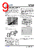
6 / 16 page  ACT4533 Rev 1, 25-Feb-13 Innovative Power TM - 6 - www.active-semi.com Copyright © 2013 Active-Semi, Inc. APPLICATIONS INFORMATION Output Voltage Setting Figure 1: Output Voltage Setting Figure 1 shows the connections for setting the output voltage. Select the proper ratio of the two feedback resistors RFB1 and RFB2 based on the output voltage. Adding a capacitor in parallel with RFB1 helps the system stability. Typically, RFB2 ≈ 10kΩ and determine RFB1 from the equation: CC Current Setting ACT4533 constant current value is set by a resistor connected between the ISET pin and GND. The CC output current is linearly proportional to the current flowing out of the ISET pin. The voltage at ISET is roughly 1V and the current gain from ISET to output is roughly 25000 (25mA/1µA). To determine the proper resistor for a desired current, please refer to Figure 2 below. Figure 2: Curve for Programming Output CC Current CC Current Line Compensation When operating at constant current mode, the current limit increase slightly with input voltage. For wide input voltage applications, a resistor RC is added to compensate line change and keep output high CC accuracy, as shown in Figure 3. Figure 3: Iutput Line Compensation Inductor Selection The inductor maintains a continuous current to the output load. This inductor current has a ripple that is dependent on the inductance value: Higher inductance reduces the peak-to-peak ripple current. The trade off for high inductance value is the increase in inductor core size and series resistance, and the reduction in current handling capability. In general, select an inductance value L based on ripple current requirement: where VIN is the input voltage, VOUT is the output voltage, fSW is the switching frequency, ILOADMAX is the maximum load current, and KRIPPLE is the ripple factor. Typically, choose KRIPPLE = 30% to correspond to the peak-to-peak ripple current being 30% of the maximum load current. With a selected inductor value the peak-to-peak inductor current is estimated as: The peak inductor current is estimated as: (3) ( ) SW IN OUT IN OUT PK LPK f V L V V V I × × × = _ _ PK LPK LOADMAX LPK _ I 2 1 I I + = (4) Output Current vs. RISET 3000 2500 2000 1500 1000 500 0 3500 RISET (kΩ) 8 11 14 17 20 23 26 29 32 VIN = 24V, VOUT = 4V (2) ( ) RIPPLE LOADMAX SW IN OUT IN OUT K I f V V V V L _ × = ⎟ ⎠ ⎞ ⎜ ⎝ ⎛ − = 1 V 808 . 0 V R R OUT 2 FB 1 FB (1) |
|
|
リンク URL |
| ALLDATASHEETはお客様のビジネスに役立ちますか? [ DONATE ] |
Alldatasheetは | 広告 | お問い合わせ | プライバシーポリシー | データシートへのリンク | リンク交換 | メーカーリスト All Rights Reserved©Alldatasheet.com |
| Russian : Alldatasheetru.com | Korean : Alldatasheet.co.kr | Spanish : Alldatasheet.es | French : Alldatasheet.fr | Italian : Alldatasheetit.com Portuguese : Alldatasheetpt.com | Polish : Alldatasheet.pl | Vietnamese : Alldatasheet.vn Indian : Alldatasheet.in | Mexican : Alldatasheet.com.mx | British : Alldatasheet.co.uk | New Zealand : Alldatasheet.co.nz |
|
Family Site : ic2ic.com |
icmetro.com |
 Japanese ▼
 English
 Chinese
 German
 Japanese
 Russian
 Korean
 Spanish
 French
 Italian
 Portuguese
 Polish
 Vietnamese
 Indian
 Mexican
 British
 New Zealand