 |
データシートサーチシステム |
|
|
データシートサーチシステム |
|
The question interval is too short.
Please try again in a few seconds.

Hello, Please ask a question about USRB02G-S08-R Datasheet
# Example questions:
➢ Referring to the 'typical application circuit', identify the purpose of components c1 and c what role do they play in the overall circuit function?
➢ Describe two of these protection features and explain how they contribute to system reliability.
➢ What primary benefits does the utc usrb02 offer compared to traditional flyback power supply designs?
| Part No. | USRB02G-S08-R |
| Manufacturer | UTC |
| Size | 224 Kbytes |
| Pages | 7 pages |
| Description | HIGH PRECISION CC/CV PRIMARY-SIDE PWM POWER SWITCH |

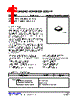




# USRB02 Preliminary LINEAR INTEGRATED CIRCUIT
## HIGH PRECISION CC/CV PRIMARY SIDE SWITCH
Description
️· Primary controller for charger/adapter applications.
️· Primary-side sensing and regulation - eliminates opto-coupler and TL431.
️· Operates in PFM (CC mode, large load) and PWM (frequency reduction, light/medium load).
️· High precision CV/CC regulation and high power efficiency.
️· Comprehensive protection features with auto-recovery.
Features
️· ±5% constant voltage regulation.
️· Primary side control (no TL431 or opto-coupler).
️· High precision constant current regulation.
️· Programmable CV and CC regulation.
️· Eliminates loop compensation circuitry.
️· Flyback topology in DCM operation.
️· Random frequency modulation (EMI reduction).
️· Built-in power NPN.
️· Multi-mode operation for efficiency.
️· Programmable cable drop compensation.
️· Built-in leading edge blanking, primary winding/line voltage compensation.
️· Audio noise free operation.
️· Open/short/over voltage/over temperature protection.
Ordering Information
️· USRB02G-S08-R: SOP-8 package, Tape Reel packing.
Pin Configuration
️· 1: VDD (Power Supply)
️· 2: FB (Voltage Feedback)
️· 3: NC (No Connect)
️· 4: CS (Current Sense Input)
️· 5-6: C (Collector of Power NPN)
️· 7-8: GND (Ground)
Absolute Maximum Ratings
️· VDD: -0.3 to 30V
️· C: -0.3 to 700V
️· CS/FB: -0.3 to 7V
️· TJ: -40 to 150°C
️· TSTG: -55 to 150°C
️· TOPR: 260°C (10 sec)
Electrical Characteristics (TA=25°C, VDD=15V)
️· IST (Startup Current): 5-15 μA
️· IOP (Static Current): 0.72-1.0 mA
️· VTH(OFF) (Turn-off Threshold): 6.5-7.8V
️· VTH(ON) (Turn-on Threshold): 18.4-20.4V
️· VDD_OVP (VDD Over Protect): 26.5-29.5V
️· TLEB (LEB Time): 0.5μS
️· VFB (Reference Voltage): 2.475-2.525V
️· F_min (Minimum Frequency): 720-880 Hz
️· T_otp (Over Temp Protection): 165°C
Operation Description
️· Startup: Low startup current; internal circuit disabled at VTH(ON).
️· CV Operation: Regulates output voltage via auxiliary winding feedback.
️· CC Operation: Maintains fixed inductance de-magnetization time; output current adjustable via Rcs.
️· Cable Drop Compensation: Internal offset voltage compensates for cable voltage drop.
️· Protection: VDD overvoltage, output overvoltage, OTP, feedback loop open, short circuit, leading edge blanking, UVLO.
Typical Application
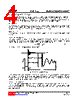
️· 5V/1A Charger/Adapter (BOM provided)
# USRB02 Preliminary LINEAR INTEGRATED CIRCUIT
## HIGH PRECISION CC/CV PRIMARY SIDE SWITCH
Description
️· Primary controller for charger/adapter applications.
️· Primary-side sensing and regulation - eliminates opto-coupler and TL431.
️· Operates in PFM (CC mode, large load) and PWM (frequency reduction, light/medium load).
️· High precision CV/CC regulation and high power efficiency.
️· Comprehensive protection features with auto-recovery.
Features
️· ±5% constant voltage regulation.
️· Primary side control (no TL431 or opto-coupler).
️· High precision constant current regulation.
️· Programmable CV and CC regulation.
️· Eliminates loop compensation circuitry.
️· Flyback topology in DCM operation.
️· Random frequency modulation (EMI reduction).
️· Built-in power NPN.
️· Multi-mode operation for efficiency.
️· Programmable cable drop compensation.
️· Built-in leading edge blanking, primary winding/line voltage compensation.
️· Audio noise free operation.
️· Open/short/over voltage/over temperature protection.
Ordering Information
️· USRB02G-S08-R: SOP-8 package, Tape Reel packing.
Pin Configuration
️· 1: VDD (Power Supply)
️· 2: FB (Voltage Feedback)
️· 3: NC (No Connect)
️· 4: CS (Current Sense Input)
️· 5-6: C (Collector of Power NPN)
️· 7-8: GND (Ground)
Absolute Maximum Ratings
️· VDD: -0.3 to 30V
️· C: -0.3 to 700V
️· CS/FB: -0.3 to 7V
️· TJ: -40 to 150°C
️· TSTG: -55 to 150°C
️· TOPR: 260°C (10 sec)
Electrical Characteristics (TA=25°C, VDD=15V)
️· IST (Startup Current): 5-15 μA
️· IOP (Static Current): 0.72-1.0 mA
️· VTH(OFF) (Turn-off Threshold): 6.5-7.8V
️· VTH(ON) (Turn-on Threshold): 18.4-20.4V
️· VDD_OVP (VDD Over Protect): 26.5-29.5V
️· TLEB (LEB Time): 0.5μS
️· VFB (Reference Voltage): 2.475-2.525V
️· F_min (Minimum Frequency): 720-880 Hz
️· T_otp (Over Temp Protection): 165°C
Operation Description
️· Startup: Low startup current; internal circuit disabled at VTH(ON).
️· CV Operation: Regulates output voltage via auxiliary winding feedback.
️· CC Operation: Maintains fixed inductance de-magnetization time; output current adjustable via Rcs.
️· Cable Drop Compensation: Internal offset voltage compensates for cable voltage drop.
️· Protection: VDD overvoltage, output overvoltage, OTP, feedback loop open, short circuit, leading edge blanking, UVLO.
Typical Application
️· 5V/1A Charger/Adapter (BOM provided)
| Part No. | USRB02G-S08-R |
| Manufacturer | UTC |
| Size | 224 Kbytes |
| Pages | 7 pages |
| Description | HIGH PRECISION CC/CV PRIMARY-SIDE PWM POWER SWITCH |
| ALLDATASHEETはお客様のビジネスに役立ちますか? [ DONATE ] |
Alldatasheetは | 広告 | お問い合わせ | プライバシーポリシー | データシートへのリンク | リンク交換 | メーカーリスト All Rights Reserved©Alldatasheet.com |
| Russian : Alldatasheetru.com | Korean : Alldatasheet.co.kr | Spanish : Alldatasheet.es | French : Alldatasheet.fr | Italian : Alldatasheetit.com Portuguese : Alldatasheetpt.com | Polish : Alldatasheet.pl | Vietnamese : Alldatasheet.vn Indian : Alldatasheet.in | Mexican : Alldatasheet.com.mx | British : Alldatasheet.co.uk | New Zealand : Alldatasheet.co.nz |
|
Family Site : ic2ic.com |
icmetro.com |
 Japanese ▼
  English
 Chinese
 German
 Russian
 Korean
 Spanish
 French
 Italian
 Portuguese
 Polish
 Vietnamese
 Indian
 Mexican
 British
 New Zealand