|
データシートサーチシステム |
|
|
データシートサーチシステム |
|
USRB02G-S08-R データシート(PDF) 5 Page - Unisonic Technologies |
|
|
|||||||||||||||||||||||||||||
USRB02G-S08-R データシート(HTML) 5 Page - Unisonic Technologies |
|
|
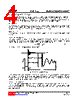
5 / 7 page  USRB02 Preliminary ` LINEAR INTEGRATED CIRCUIT UNISONICTECHNOLOGIESCO.,LTD 5 of 7 www.unisonic.com.tw QW-R103-087.a OPERATION DESCRIPTION (Cont.) Iout Vout Large Rcs Small Rcs Figure3. Adjustable output power by changing Rcs Figure4. Secondary current waveform In CC operation, the CC loop control function of UTC USRB02 will keep a fixed proportion between secondary inductance de-magnetization time (Tdemag) and switching cycle time (Tsw). The fixed proportion is 2 1 = T T SW demag (2) Thus the output current is given by: PK S P SW demag PK S P out I × N N × 4 1 = T T × I × N N × 2 1 = I (3) Programmable Cable drop Compensation UTC USRB02 has a built-in cable voltage drop compensation to achieve good load regulation. An offset voltage is generated at FB pin by an internal current flowing into the resistor divider. it is inversely proportional to the output load current. The voltage drop across the cable is compensated by this offset voltage at FB pin. It can also be programmed by adjusting the resistance of the divider to compensate the drop for various cable lines used. Current Sensing and Leading Edge Blanking Cycle-by-cycle current limiting is offered in UTC USRB02. The switch current is detected by a sense resistor into the CS pin. When the power switch is turned on, a turn-on spike will occur on this resistor. A 500ns leading-edge blanking is built in to avoid false-termination of the switching pulse so that the external RC filtering is no longer needed. |
|
|
リンク URL |
| ALLDATASHEETはお客様のビジネスに役立ちますか? [ DONATE ] |
Alldatasheetは | 広告 | お問い合わせ | プライバシーポリシー | データシートへのリンク | リンク交換 | メーカーリスト All Rights Reserved©Alldatasheet.com |
| Russian : Alldatasheetru.com | Korean : Alldatasheet.co.kr | Spanish : Alldatasheet.es | French : Alldatasheet.fr | Italian : Alldatasheetit.com Portuguese : Alldatasheetpt.com | Polish : Alldatasheet.pl | Vietnamese : Alldatasheet.vn Indian : Alldatasheet.in | Mexican : Alldatasheet.com.mx | British : Alldatasheet.co.uk | New Zealand : Alldatasheet.co.nz |
|
Family Site : ic2ic.com |
icmetro.com |
 Japanese ▼
 English
 Chinese
 German
 Japanese
 Russian
 Korean
 Spanish
 French
 Italian
 Portuguese
 Polish
 Vietnamese
 Indian
 Mexican
 British
 New Zealand