|
データシートサーチシステム |
|
|
データシートサーチシステム |
|
LP6303 データシート(PDF) 10 Page - Lowpower Semiconductor inc |
|
|
|||||||||||||||||||||||||||||
LP6303 データシート(HTML) 10 Page - Lowpower Semiconductor inc |
|
|
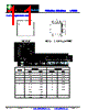
10 / 11 page  LP6303-01 Apr.-2014 Email: marketing@lowpowersemi.com www.lowpowersemi.com Page 10 of 11 Preliminary Datasheet LP6303 PCB Layout Layout is very critical for PMIC designs. For LP6303 PCB layout considerations, please refer to the following suggestions to get best performance. It is suggested to use 4-layer PCB layout and place LX plane and output plane on the top layer, place VIN plane in the inner layer. The top layer SMD input and output capacitors ground plane should be connected to the internal ground layer and bottom ground plane individually by using vias. The GND should be connected to inner ground layer directly by using via. High current path traces need to be widened. Place the input capacitors as close as possible to the VINx pin to reduce noise interference. Keep the feedback path (from VOUTX to FBx) away from the noise node (ex. LXx). LXx is a high current noise node. Complete the layout by using short and wide traces. The top layer exposed pad ground plane should be connected to the internal ground layer and bottom ground plane by using a number of vias to improve thermal performance. Place the input capacitors as close as possible to the VINx pin to reduce noise interference. |
|
|
リンク URL |
| ALLDATASHEETはお客様のビジネスに役立ちますか? [ DONATE ] |
Alldatasheetは | 広告 | お問い合わせ | プライバシーポリシー | データシートへのリンク | リンク交換 | メーカーリスト All Rights Reserved©Alldatasheet.com |
| Russian : Alldatasheetru.com | Korean : Alldatasheet.co.kr | Spanish : Alldatasheet.es | French : Alldatasheet.fr | Italian : Alldatasheetit.com Portuguese : Alldatasheetpt.com | Polish : Alldatasheet.pl | Vietnamese : Alldatasheet.vn Indian : Alldatasheet.in | Mexican : Alldatasheet.com.mx | British : Alldatasheet.co.uk | New Zealand : Alldatasheet.co.nz |
|
Family Site : ic2ic.com |
icmetro.com |
 Japanese ▼
 English
 Chinese
 German
 Japanese
 Russian
 Korean
 Spanish
 French
 Italian
 Portuguese
 Polish
 Vietnamese
 Indian
 Mexican
 British
 New Zealand