|
データシートサーチシステム |
|
|
データシートサーチシステム |
|
AD8337BCPZ-R2 データシート(PDF) 6 Page - Analog Devices |
|
|
|||||||||||||||||||||||||||||
AD8337BCPZ-R2 データシート(HTML) 6 Page - Analog Devices |
|
|
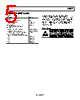
6 / 28 page  AD8337 Data Sheet Rev. D | Page 6 of 28 PIN CONFIGURATION AND FUNCTION DESCRIPTIONS INPN VOUT VCOM INPP VPOS PRAO VNEG GAIN NOTES 1. FOR BEST THERMAL PERFORMANCE, EXPOSED PAD MUST BE SOLDERED TO PCB. 3 4 1 2 6 5 8 7 AD8337 TOP VIEW (Not to Scale) Figure 2. Pin Configuration Table 3. Pin Function Descriptions Pin No. Mnemonic Description 1 VOUT VGA Output. 2 VCOM Common Ground When Using Plus and Minus Supply Voltages. For single-supply operation, provide half the positive supply voltage at the VPOS pin to VCOM pin. 3 INPP Positive Input to Preamplifier. 4 INPN Negative Input to Preamplifier. 5 PRAO Preamplifier Output. 6 VNEG Negative Supply (−VPOS for Dual Supply; GND for Single Supply). 7 GAIN Gain Control Input Centered at VCOM. 8 VPOS Positive Supply. EP Exposed Pad For best thermal performance, exposed pad must be soldered to PCB. |
|
|
リンク URL |
| ALLDATASHEETはお客様のビジネスに役立ちますか? [ DONATE ] |
Alldatasheetは | 広告 | お問い合わせ | プライバシーポリシー | データシートへのリンク | リンク交換 | メーカーリスト All Rights Reserved©Alldatasheet.com |
| Russian : Alldatasheetru.com | Korean : Alldatasheet.co.kr | Spanish : Alldatasheet.es | French : Alldatasheet.fr | Italian : Alldatasheetit.com Portuguese : Alldatasheetpt.com | Polish : Alldatasheet.pl | Vietnamese : Alldatasheet.vn Indian : Alldatasheet.in | Mexican : Alldatasheet.com.mx | British : Alldatasheet.co.uk | New Zealand : Alldatasheet.co.nz |
|
Family Site : ic2ic.com |
icmetro.com |
 Japanese ▼
 English
 Chinese
 German
 Japanese
 Russian
 Korean
 Spanish
 French
 Italian
 Portuguese
 Polish
 Vietnamese
 Indian
 Mexican
 British
 New Zealand