|
データシートサーチシステム |
|
|
データシートサーチシステム |
|
M8870-R3 データシート(PDF) 4 Page - Clare, Inc. |
|
|
|||||||||||||||||||||||||||||
M8870-R3 データシート(HTML) 4 Page - Clare, Inc. |
|
|
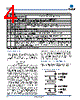
4 / 9 page  Pin Functions Pin Name Description 1 IN+ Non-inverting input Connections to the front-end differential amplifier. 2 IN- Inverting input 3 GS Gain select. Gives access to output of front-end amplifier for connection of feedback resistor. 4V REF Reference voltage output (nominally VDD/2). May be used to bias the inputs at mid-rail. 5 INH* Inhibits detection of tones representing keys A, B, C, and D. 6 PD* Power down. Logic high powers down the device and inhibits the oscillator. Internal pulldown. 7 OSC1 Clock input 3.579545 MHz crystal connected between these pins completes the internal oscillator. 8 OSC2 Clock output 9 VSS Negative power supply (normally connected to 0 V). 10 OE Tri-statable output enable (input). Logic high enables the outputs Q1 - Q4. Internal pullup. 11-14 Q1, Q2, Tri-statable data outputs. When enabled by OE, provides the code corresponding to the last valid tone pair Q3, Q4 received (see Tone Decoding table on page 5). 15 StD Delayed steering output. Presents a logic high when a received tone pair has been registered and the output latch is updated. Returns to logic low when the voltage on St/GT falls below VTSt. 16 ESt Early steering output. Presents a logic high immediately when the digital algorithm detects a recognizable tone pair (signal condition). Any momentary loss of signal condition will cause ESt to return to a logic low. 17 St/GT Steering input/guard time output (bidirectional). A voltage greater than VTSt detected at St causes the device to register the detected tone pair and update the output latch. A voltage less than VTSt frees the device to accept a new tone pair. The GT output acts to reset the external steering time constant, and its state is a function of ESt and the voltage on St. (See Common Crystal Connection on page 5). 18 V DD Positive power supply. (Normally connected to +5V.) * -02 only. Connect to V SS for -01 version www.clare.com 4 M-8870 Rev. 3 Guard Time Adjustment Where independent selection of signal duration and interdigit pause are not required, the simple steering circuit of Basic Steering Circuit is applicable. Component values are chosen according to the formu- la: t REC = tDP + tGTP t GTP @ 0.67 RC The value of tDP is a parameter of the device and tREC is the minimum signal duration to be recognized by the receiver. A value for C of 0.1 µF is recommend- ed for most applications, leaving R to be selected by the designer. For example, a suitable value of R for a t REC of 40 ms would be 300 kΩ. A typical circuit using this steering configuration is shown in the Single - Ended Input Configuration on page 4. The timing requirements for most telecommunication applications are satisfied with this circuit. Different steering arrange- ments may be used to select independently the guard times for tone-present (t GTP) and tone-absent (tGTA). This may be necessary to meet system specifications that place both accept and reject limits on both tone duration and interdigit pause. Guard time adjustment also allows the designer to tai- lor system parameters such as talkoff and noise immu- nity. Increasing t REC improves talkoff performance, since it reduces the probability that tones simulated by speech will maintain signal condition long enough to be registered. On the other hand, a relatively short t REC with a long t DO would be appropriate for extremely noisy environments where fast acquisition time and immunity to dropouts would be required. Design infor- mation for guard time adjustment is shown in the Guard Time Adjustment below. Power-down and Inhibit Mode (-02 only) A logic high applied to pin 6 (PD) will place the device into standby mode to minimize power consumption. It Figure 5 Guard Time Adjustment |
|
|
リンク URL |
| ALLDATASHEETはお客様のビジネスに役立ちますか? [ DONATE ] |
Alldatasheetは | 広告 | お問い合わせ | プライバシーポリシー | データシートへのリンク | リンク交換 | メーカーリスト All Rights Reserved©Alldatasheet.com |
| Russian : Alldatasheetru.com | Korean : Alldatasheet.co.kr | Spanish : Alldatasheet.es | French : Alldatasheet.fr | Italian : Alldatasheetit.com Portuguese : Alldatasheetpt.com | Polish : Alldatasheet.pl | Vietnamese : Alldatasheet.vn Indian : Alldatasheet.in | Mexican : Alldatasheet.com.mx | British : Alldatasheet.co.uk | New Zealand : Alldatasheet.co.nz |
|
Family Site : ic2ic.com |
icmetro.com |
 Japanese ▼
 English
 Chinese
 German
 Japanese
 Russian
 Korean
 Spanish
 French
 Italian
 Portuguese
 Polish
 Vietnamese
 Indian
 Mexican
 British
 New Zealand