|
データシートサーチシステム |
|
|
データシートサーチシステム |
|
CAT310 データシート(PDF) 7 Page - Catalyst Semiconductor |
|
|
|||||||||||||||||||||||||||||
CAT310 データシート(HTML) 7 Page - Catalyst Semiconductor |
|
|
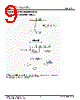
7 / 10 page  CAT310 © 2005 Catalyst Semiconductor, Inc. 7 Doc No. 25087, Rev. 00 Characteristics subject to change without notice FUNCTIONAL DESCRIPTION The CAT310 implements a 10-bit serial-in shift register for storing the setting of the ten outputs. Serial input data SIN are clocked into the shift register on the rising edge of the clock. At the 10th clock pulse, the first data bit entered is outputted from the shift register to SOUT. The following clock pulses will output the following data bits onto SOUT. The output data pattern replicates the input data stream with a delay of ten clock pulses. The 10-bit data pattern present in the shift register is stored in the 10-bit data latch when the latch signal XLAT is logic high. When XLAT transitions to logic low, data are latched and stay unchanged for as long as XLAT remains low. The last serial input data corresponds to OUT0. The serial input data that was received 10 clock pulse ago is stored in OUT9. When the BLANK input is logic high, all the output switches are in the off state. If the BLANK input is low, the 10-bit data latches control the 10 output switches. A data bit value of zero keeps the switch off. A data bit value of one keeps the switch on. Serial to Parallel Shift Register CLK → SIN → Bit 0 Bit 1 Bit 2 Bit 3 Bit 4 Bit 5 Bit 6 Bit 7 Bit 8 Bit 9 → SOUT Data Latch ↓ ↓ ↓ ↓ ↓ ↓ ↓ ↓ ↓ ↓ XLAT → LED OUT0 LED OUT1 LED OUT2 LED OUT3 LED OUT4 LED OUT5 LED OUT6 LED OUT7 LED OUT8 LED OUT9 TIMING DIAGRAM |
|
|
リンク URL |
| ALLDATASHEETはお客様のビジネスに役立ちますか? [ DONATE ] |
Alldatasheetは | 広告 | お問い合わせ | プライバシーポリシー | データシートへのリンク | リンク交換 | メーカーリスト All Rights Reserved©Alldatasheet.com |
| Russian : Alldatasheetru.com | Korean : Alldatasheet.co.kr | Spanish : Alldatasheet.es | French : Alldatasheet.fr | Italian : Alldatasheetit.com Portuguese : Alldatasheetpt.com | Polish : Alldatasheet.pl | Vietnamese : Alldatasheet.vn Indian : Alldatasheet.in | Mexican : Alldatasheet.com.mx | British : Alldatasheet.co.uk | New Zealand : Alldatasheet.co.nz |
|
Family Site : ic2ic.com |
icmetro.com |
 Japanese ▼
 English
 Chinese
 German
 Japanese
 Russian
 Korean
 Spanish
 French
 Italian
 Portuguese
 Polish
 Vietnamese
 Indian
 Mexican
 British
 New Zealand