|
データシートサーチシステム |
|
|
データシートサーチシステム |
|
IS25LP032D-RBLE:P データシート(PDF) 50 Page - Integrated Silicon Solution, Inc |
|
|
|||||||||||||||||||||||||||||
IS25LP032D-RBLE:P データシート(HTML) 50 Page - Integrated Silicon Solution, Inc |
|
|
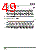
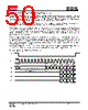
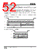
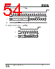
50 / 118 page  IS25LP032D IS25WP032D Integrated Silicon Solution, Inc.- www.issi.com 50 Rev. A12 08/04/2020 8.9 QUAD INPUT PAGE PROGRAM OPERATION (PPQ, 32h/38h) The Quad Input Page Program instruction allows up to 256 bytes data to be programmed into memory in a single operation with four pins (IO0, IO1, IO2 and IO3). The destination of the memory to be programmed must be outside the protected memory area set by the Block Protection (BP3, BP2, BP1, BP0) bits. A Quad Input Page Program instruction which attempts to program into a page that is write-protected will be ignored. Before the execution of Quad Input Page Program instruction, the QE bit in the Status Register must be set to “1” and the Write Enable Latch (WEL) must be enabled through a Write Enable (WREN) instruction. Program operation will start immediately after the CE# is brought high, otherwise the Quad Input Page Program instruction will not be executed. The internal control logic automatically handles the programming voltages and timing. The progress or completion of the program operation can be determined by reading the WIP bit in Status Register via a RDSR instruction. If the WIP bit is “1”, the program operation is still in progress. If WIP bit is “0”, the program operation has completed. If more than 256 bytes data are sent to a device, the address counter rolls over within the same page, the previously latched data are discarded, and the last 256 bytes data are kept to be programmed into the page. The starting byte can be anywhere within the page. When the end of the page is reached, the address will wrap around to the beginning of the same page. If the data to be programmed are less than a full page, the data of all other bytes on the same page will remain unchanged. Note: A program operation can alter “1”s into “0”s. The same byte location or page may be programmed more than once, to incrementally change “1”s to “0”s. An erase operation is required to change “0”s to “1”s. Figure 8.13 Quad Input Page Program Sequence Instruction = 32h/38h 23 CE # SCK 4 0 4 0 3-byte Address High Impedance 22 ... 0 0 1 2 3 4 5 6 7 8 9 31 32 33 34 35 Mode 3 Mode 0 IO0 IO1 5 1 5 1 6 2 6 2 7 3 7 3 Data In 2 IO2 IO3 ... Data In 1 ... ... ... ... ... |
|
リンク URL |
| ALLDATASHEETはお客様のビジネスに役立ちますか? [ DONATE ] |
Alldatasheetは | 広告 | お問い合わせ | プライバシーポリシー | データシートへのリンク | リンク交換 | メーカーリスト All Rights Reserved©Alldatasheet.com |
| Russian : Alldatasheetru.com | Korean : Alldatasheet.co.kr | Spanish : Alldatasheet.es | French : Alldatasheet.fr | Italian : Alldatasheetit.com Portuguese : Alldatasheetpt.com | Polish : Alldatasheet.pl | Vietnamese : Alldatasheet.vn Indian : Alldatasheet.in | Mexican : Alldatasheet.com.mx | British : Alldatasheet.co.uk | New Zealand : Alldatasheet.co.nz |
|
Family Site : ic2ic.com |
icmetro.com |
 Japanese ▼
 English
 Chinese
 German
 Japanese
 Russian
 Korean
 Spanish
 French
 Italian
 Portuguese
 Polish
 Vietnamese
 Indian
 Mexican
 British
 New Zealand