|
データシートサーチシステム |
|
|
データシートサーチシステム |
|
IS25LP032D-RKLE:P データシート(PDF) 39 Page - Integrated Silicon Solution, Inc |
|
|
|||||||||||||||||||||||||||||
IS25LP032D-RKLE:P データシート(HTML) 39 Page - Integrated Silicon Solution, Inc |
|
|
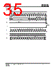
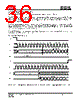
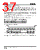
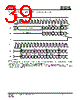
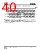
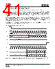
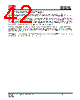
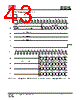
39 / 118 page  IS25LP032D IS25WP032D Integrated Silicon Solution, Inc.- www.issi.com 39 Rev. A12 08/04/2020 Figure 8.4 Fast Read Dual I/O Sequence (with command decode cycles) 7 5 3 7 5 1 3 1 Data Out 1 Instruction = BBh 22 CE # SCK 2 0 6 4 3-byte Address High Impedance 20 18 ... 0 1 2 3 4 5 6 7 8 9 10 ... 18 19 20 21 22 23 24 25 26 27 28 29 30 31 32 33 34 35 36 37 Mode 3 Mode 0 ... tV 23 3 1 7 5 21 19 ... IO0 IO1 3 1 2 0 6 4 2 6 4 0 2 0 4 Dummy Cycles 7 5 3 1 6 4 2 0 7 5 ... 6 4 ... CE # SCK IO0 IO1 Data Out 2 Data Out 3 Mode Bits Mode Bits Notes: 1. If the mode bits=AXh ( where X is don’t care), it can execute the AX read mode (without command). When the mode bits are different from AXh, the device exits the AX read operation. 2. Number of dummy cycles depends on clock speed. Detailed information in Table 6.11 Read Dummy Cycles. 3. Sufficient dummy cycles are required to avoid I/O contention. If the number of dummy cycles and AX bit cycles are same, then X should be Hi-Z. |
|
リンク URL |
| ALLDATASHEETはお客様のビジネスに役立ちますか? [ DONATE ] |
Alldatasheetは | 広告 | お問い合わせ | プライバシーポリシー | データシートへのリンク | リンク交換 | メーカーリスト All Rights Reserved©Alldatasheet.com |
| Russian : Alldatasheetru.com | Korean : Alldatasheet.co.kr | Spanish : Alldatasheet.es | French : Alldatasheet.fr | Italian : Alldatasheetit.com Portuguese : Alldatasheetpt.com | Polish : Alldatasheet.pl | Vietnamese : Alldatasheet.vn Indian : Alldatasheet.in | Mexican : Alldatasheet.com.mx | British : Alldatasheet.co.uk | New Zealand : Alldatasheet.co.nz |
|
Family Site : ic2ic.com |
icmetro.com |
 Japanese ▼
 English
 Chinese
 German
 Japanese
 Russian
 Korean
 Spanish
 French
 Italian
 Portuguese
 Polish
 Vietnamese
 Indian
 Mexican
 British
 New Zealand