|
データシートサーチシステム |
|
|
データシートサーチシステム |
|
ADL5369ACPZ-R7 データシート(PDF) 5 Page - Analog Devices |
|
|
|||||||||||||||||||||||||||||
ADL5369ACPZ-R7 データシート(HTML) 5 Page - Analog Devices |
|
|
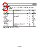
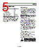
5 / 23 page  Data Sheet ADL5369 Rev. A | Page 5 of 23 ABSOLUTE MAXIMUM RATINGS Table 5. Parameter Rating VS 5.5 V RF Input Level 20 dBm LO Input Level 13 dBm IFOP, IFON Bias Voltage 6.0 V VGS0, VGS1, LOSW, PWDN 5.5 V Internal Power Dissipation 0.6 W Maximum Junction Temperature 150°C Operating Temperature Range −40°C to +85°C Storage Temperature Range −65°C to +150°C Lead Temperature (Soldering, 60 sec) 260°C Stresses at or above those listed under Absolute Maximum Ratings may cause permanent damage to the product. This is a stress rating only; functional operation of the product at these or any other conditions above those indicated in the operational section of this specification is not implied. Operation beyond the maximum operating conditions for extended periods may affect product reliability. THERMAL RESISTANCE θJA is the junction to ambient thermal resistance (°C/W), θJB is the junction to board thermal resistance (°C/W), and θJC is the junction to case thermal resistance (°C/W). θJC is determined by the mechanical design of the ADL5369 and is optimized to the lowest possible value. θJA and θJB are functions of the design of the PCB, and are under the control of the user. The data shown in Table 6 is based on a JEDEC standard design and is provided for comparison purposes. Table 6. Thermal Resistance Package Type θJA1 θJB1 θJC1 Unit 20-Lead LFCSP 25 14.74 1.08 °C/W 1 See JEDEC Standard JESD51-2 for information on optimizing thermal impedance (PCB with 3 × 3 vias). Junction to Board Thermal Impedance The junction to board thermal impedance (θJB) is the thermal impedance from the die to or near the component lead of the ADL5369. For the ADL5369, θJB was determined experimentally to be 14.74°C/W with the device mounted on a 4-layer circuit board (two of the layers being ground planes) in a configuration similar to that of the ADL5369-EVALZ evaluation board. Board size and complexity (number of layers) affect θJB; more layers tend to reduce the thermal impedance slightly. If the board temperature is known, use the junction to board thermal impedance to calculate die temperature (also known as junction temperature) to ensure that it does not exceed the speci- fied limit of 150°C. For example, if the board temperature is 85°C, the die temperature is given by the equation TJ = TB + (PDISS × θJB) where: TJ is the junction temperature. TB is the board temperature measured at or near the component lead. PDISS is the power dissipated from the device. The typical worst case power dissipation for the ADL5369 is 522 mW (5.5 V × 95 mA). Therefore, TJ is TJ = 85°C + (0.522 W × 14.74°C/W) = 92.70°C ESD CAUTION |
|
|
リンク URL |
| ALLDATASHEETはお客様のビジネスに役立ちますか? [ DONATE ] |
Alldatasheetは | 広告 | お問い合わせ | プライバシーポリシー | データシートへのリンク | リンク交換 | メーカーリスト All Rights Reserved©Alldatasheet.com |
| Russian : Alldatasheetru.com | Korean : Alldatasheet.co.kr | Spanish : Alldatasheet.es | French : Alldatasheet.fr | Italian : Alldatasheetit.com Portuguese : Alldatasheetpt.com | Polish : Alldatasheet.pl | Vietnamese : Alldatasheet.vn Indian : Alldatasheet.in | Mexican : Alldatasheet.com.mx | British : Alldatasheet.co.uk | New Zealand : Alldatasheet.co.nz |
|
Family Site : ic2ic.com |
icmetro.com |
 Japanese ▼
 English
 Chinese
 German
 Japanese
 Russian
 Korean
 Spanish
 French
 Italian
 Portuguese
 Polish
 Vietnamese
 Indian
 Mexican
 British
 New Zealand