|
データシートサーチシステム |
|
|
データシートサーチシステム |
|
AD8091ARTZ-R2 データシート(PDF) 16 Page - Analog Devices |
|
|
|||||||||||||||||||||||||||||
AD8091ARTZ-R2 データシート(HTML) 16 Page - Analog Devices |
|
|
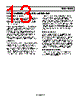
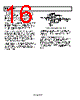
16 / 20 page  A8091/AD8092 Rev. B | Page 16 of 20 The other extreme is a full white video signal. The blanking intervals and sync tips of such a signal have negative-going excursions in compliance with the composite video specifications. The combination of horizontal and vertical blanking intervals limit such a signal to being at the highest (white) level for a maximum of about 75% of the time. AD8091 5V + 4.99k Ω 10 µF 47 µF + 4.99k Ω 10k Ω RT 75 Ω RG 1k Ω RF 1k Ω RBT 75 Ω RL 75 Ω VOUT COMPOSITE VIDEO IN + 220 µF 0.1 µF 3 2 4 6 7 1000 µF 0.1 µF10µF + As a result of the duty cycles between the two extremes, a 1 V p- p composite video signal that is multiplied by a gain of 2 requires about 3.2 V p-p of dynamic voltage swing at the output for an op amp to pass a composite video signal of arbitrary varying duty cycle without distortion. Figure 36. Single-Supply Composite Video Line Driver The feedback circuit provides unity gain for the dc biasing of the input and provides a gain of 2 for any signals that are in the video bandwidth. The output is ac-coupled and terminated to drive the line. Some circuits use a sync tip clamp to hold the sync tips at a relatively constant level to lower the amount of dynamic signal swing required. However, these circuits can have artifacts like sync tip compression unless they are driven by a source with a very low output impedance. The AD8091/AD8092 have adequate signal swing when running on a single 5 V supply to handle an ac-coupled composite video signal. The capacitor values were selected for providing minimum tilt or field time distortion of the video signal. These values would be required for video that is considered to be studio or broadcast quality. However, if a lower consumer grade of video, sometimes referred to as consumer video, is all that is desired, the values and the cost of the capacitors can be reduced by as much as a factor of 5 with minimum visible degradation in the picture. The input to the circuit in Figure 36 is a standard composite (1 V p-p) video signal that has the blanking level at ground. The input network level shifts the video signal by means of ac coupling. The noninverting input of the op amp is biased to half of the supply voltage. |
|
|
リンク URL |
| ALLDATASHEETはお客様のビジネスに役立ちますか? [ DONATE ] |
Alldatasheetは | 広告 | お問い合わせ | プライバシーポリシー | データシートへのリンク | リンク交換 | メーカーリスト All Rights Reserved©Alldatasheet.com |
| Russian : Alldatasheetru.com | Korean : Alldatasheet.co.kr | Spanish : Alldatasheet.es | French : Alldatasheet.fr | Italian : Alldatasheetit.com Portuguese : Alldatasheetpt.com | Polish : Alldatasheet.pl | Vietnamese : Alldatasheet.vn Indian : Alldatasheet.in | Mexican : Alldatasheet.com.mx | British : Alldatasheet.co.uk | New Zealand : Alldatasheet.co.nz |
|
Family Site : ic2ic.com |
icmetro.com |
 Japanese ▼
 English
 Chinese
 German
 Japanese
 Russian
 Korean
 Spanish
 French
 Italian
 Portuguese
 Polish
 Vietnamese
 Indian
 Mexican
 British
 New Zealand