|
データシートサーチシステム |
|
|
データシートサーチシステム |
|
AD8063ARTZ-R2 データシート(PDF) 18 Page - Analog Devices |
|
|
|||||||||||||||||||||||||||||
AD8063ARTZ-R2 データシート(HTML) 18 Page - Analog Devices |
|
|
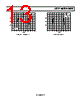
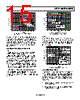
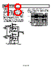
18 / 20 page  AD8061/AD8062/AD8063 Rev. D | Page 18 of 20 The SELECT signal and the output waveforms for this circuit are shown in Figure 57. For synchronization clarity, two differ- ent frequency synthesizers, whose time bases are locked to each other, generate the signals. MULTIPLEXER The AD8063 has a disable pin used to power down the ampli- fier to save power or to create a mux circuit. If two (or more) AD8063 outputs are connected together, and only one is enabled, then only the signal of the enabled amplifier will appear at the output. This configuration is used to select from various input signal sources. Additionally, the same input signal is applied to different gain stages, or differently tuned filters, to make a gain- step amplifier or a selectable frequency amplifier. 1V 2V 2 μs SELECT OUTPUT Figure 56 shows a schematic of two AD8063s used to create a mux that selects between two inputs. One of these is a 1 V p-p, 3 MHz sine wave; the other is a 2 V p-p, 1 MHz sine wave. 49.9 Ω 1k Ω +4V 1 –4V 49.9 Ω TIME BASE OUT TIME BASE IN 1V p-p 3MHz 2V p-p 1MHz VOUT 49.9 Ω SELECT HCO4 1k Ω 10 μF 0.1 μF 10 μF 0.1 μF AD8063 49.9 Ω 1k Ω +4V 1 –4V 1k Ω 10 μF 0.1 μF 10 μF 0.1 μF AD8063 Figure 57. AD8063 Mux Output Figure 56. Two-to-One Multiplexer Using Two AD8063s |
|
|
リンク URL |
| ALLDATASHEETはお客様のビジネスに役立ちますか? [ DONATE ] |
Alldatasheetは | 広告 | お問い合わせ | プライバシーポリシー | データシートへのリンク | リンク交換 | メーカーリスト All Rights Reserved©Alldatasheet.com |
| Russian : Alldatasheetru.com | Korean : Alldatasheet.co.kr | Spanish : Alldatasheet.es | French : Alldatasheet.fr | Italian : Alldatasheetit.com Portuguese : Alldatasheetpt.com | Polish : Alldatasheet.pl | Vietnamese : Alldatasheet.vn Indian : Alldatasheet.in | Mexican : Alldatasheet.com.mx | British : Alldatasheet.co.uk | New Zealand : Alldatasheet.co.nz |
|
Family Site : ic2ic.com |
icmetro.com |
 Japanese ▼
 English
 Chinese
 German
 Japanese
 Russian
 Korean
 Spanish
 French
 Italian
 Portuguese
 Polish
 Vietnamese
 Indian
 Mexican
 British
 New Zealand