|
データシートサーチシステム |
|
|
データシートサーチシステム |
|
LTM4650 データシート(PDF) 9 Page - Analog Devices |
|
|
|||||||||||||||||||||||||||||
LTM4650 データシート(HTML) 9 Page - Analog Devices |
|
|
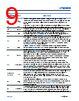
9 / 38 page  Data Sheet LTM4640 analog.com Rev. 0 9 of 38 PIN NAME DESCRIPTION CFG 1 B3 INTVCC Internal 3.3V Regulator Output of the Switching Mode Regulator Channel. The internal power drivers and control circuits are powered by this voltage. The LTM4640 has an internal 2.2µF decoupling capacitor. No external decoupling capacitor is required. B4 RUN Run Control Input Pin. Enable regulator operation by connecting the RUN pin above 1.35V. Connecting it below 1.1V shuts down the specific regulator channel. B5 PGOOD Output Power Good Pin with Open-Drain Logic. The PGOOD pin is pulled to ground when the voltage on the FB pin is out of ±8% of the internal 0.6V reference. B7 SW Switching node of each channel that is used for testing purposes. Also, an R-C snubber network is applied to reduce or eliminate switch node ringing. Otherwise, leave it floating. See the Applications Information section for details. C1 FB The Negative Input of the Error Amplifier for the Switching Mode Regulator. This pin is internally connected to VOSNS+ with a 10kΩ precision resistor. The output voltage is programmed with an additional resistor between FB and VOSNS– pins. In a PolyPhase® operation, connect the FB pins together to allow for a parallel operation. See the Applications Information section for details. C2 VOSNS– Negative Input to the Differential Remote Sense Amplifier. Connect an external resistor between FB and VOSNS– pins to set the output voltage of the specific channel. See the Applications Information section for details. D1 COMPa Current control threshold and error amplifier compensation point of the switching mode regulator channel. The internal current comparator threshold is linearly proportional to this voltage. Connect the COMPa pins from different channels together for a parallel operation. The device is internally compensated. Connect to the COMPb pin to use the internal compensation. Or connect to a Type-II C-R-C network to use customized compensation. D2 MODE/CLKIN Discontinuous Mode Select Pin and External Synchronization Input to Phase Detector. Connect MODE/CLKIN to GND for discontinuous-conduction mode (DCM) operation. Floating MODE/CLKIN or connecting it to a voltage above 1V selects forced continuous mode (FCM). Furthermore, connecting MODE/CLKIN to an external clock synchronizes the system clock to the external clock and puts the part in FCM. See the Applications Information section for details. D3–D4, E3– E4, F4, G4 VIN Power input pins connect to the drain of the internal top MOSFET, and the signal VIN to the internal 3.3V regulator for the control circuitry for each switching mode regulator channel. Apply input voltages between these pins and GND pins. Recommend placing input decoupling capacitance directly between each of the VIN pins and the GND pins. E1 FREQ Switching Frequency Program Pin. The frequency is set internally to 600kHz. An external resistor is placed from this pin to GND to increase frequency, or from this pin to INTVCC to reduce frequency. See the Applications Information section for frequency adjustment. E2 TRACK/SS Output Tracking and Soft Start Pin of the Switching Mode Regulator. The TRACK/SS pin allows the user to control the rise time of the output voltage. Putting a voltage below 0.6V on this pin bypasses the internal reference input to the error amplifier, instead it servos the FB pin to the TRACK voltage. Above 0.6V, the tracking function |
|
リンク URL |
| ALLDATASHEETはお客様のビジネスに役立ちますか? [ DONATE ] |
Alldatasheetは | 広告 | お問い合わせ | プライバシーポリシー | データシートへのリンク | リンク交換 | メーカーリスト All Rights Reserved©Alldatasheet.com |
| Russian : Alldatasheetru.com | Korean : Alldatasheet.co.kr | Spanish : Alldatasheet.es | French : Alldatasheet.fr | Italian : Alldatasheetit.com Portuguese : Alldatasheetpt.com | Polish : Alldatasheet.pl | Vietnamese : Alldatasheet.vn Indian : Alldatasheet.in | Mexican : Alldatasheet.com.mx | British : Alldatasheet.co.uk | New Zealand : Alldatasheet.co.nz |
|
Family Site : ic2ic.com |
icmetro.com |
 Japanese ▼
 English
 Chinese
 German
 Japanese
 Russian
 Korean
 Spanish
 French
 Italian
 Portuguese
 Polish
 Vietnamese
 Indian
 Mexican
 British
 New Zealand