|
データシートサーチシステム |
|
|
データシートサーチシステム |
|
TPD1018F データシート(PDF) 2 Page - Toshiba Semiconductor |
|
|
|||||||||||||||||||||||||||||
TPD1018F データシート(HTML) 2 Page - Toshiba Semiconductor |
|
|
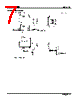
2 / 8 page  TPD1018F 2006-10-31 2 Pin Description Pin No. Symbol Function 1 OUT Output pin. When the load is short-circuited and current in excess of the detection current (0.5A min) flows to the output pin, the current limiter operates to protect the IC. 2, 3, 4 GND Ground pins. 5 VDD Power pin. Incorporates an overvoltage protection function which turns off the output when the voltage applied exceeds 25V (min). Protects IC and load. Incorporates 2V (typ.) hysteresis. 6 IN Input is CMOS-compatible, with pull-down resistor connected. Even if the input is open, output will not accidentally turn on. 7, 8, 9 GND Ground pins. 10 DIAG Self-diagnosis detection pin. Goes low when overcurrent, overheating, or overvoltage is detected. n-channel open drain. Timing Chart Truth Table Input Signal Output Signal Diagnosis Output State H H H L L H Normal H L L L L H Overcurrent H L L L L H Overtemperature H L L L L H Overvoltage |
|
|
リンク URL |
| ALLDATASHEETはお客様のビジネスに役立ちますか? [ DONATE ] |
Alldatasheetは | 広告 | お問い合わせ | プライバシーポリシー | データシートへのリンク | リンク交換 | メーカーリスト All Rights Reserved©Alldatasheet.com |
| Russian : Alldatasheetru.com | Korean : Alldatasheet.co.kr | Spanish : Alldatasheet.es | French : Alldatasheet.fr | Italian : Alldatasheetit.com Portuguese : Alldatasheetpt.com | Polish : Alldatasheet.pl | Vietnamese : Alldatasheet.vn Indian : Alldatasheet.in | Mexican : Alldatasheet.com.mx | British : Alldatasheet.co.uk | New Zealand : Alldatasheet.co.nz |
|
Family Site : ic2ic.com |
icmetro.com |
 Japanese ▼
 English
 Chinese
 German
 Japanese
 Russian
 Korean
 Spanish
 French
 Italian
 Portuguese
 Polish
 Vietnamese
 Indian
 Mexican
 British
 New Zealand