|
データシートサーチシステム |
|
|
データシートサーチシステム |
|
AD8647ARMZ-R2 データシート(PDF) 15 Page - Analog Devices |
|
|
|||||||||||||||||||||||||||||
AD8647ARMZ-R2 データシート(HTML) 15 Page - Analog Devices |
|
|
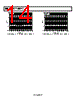
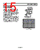
15 / 20 page  AD8646/AD8647/AD8648 Rev. B | Page 15 of 20 THEORY OF OPERATION POWER-DOWN OPERATION The shutdown function of the AD8647 is referenced to the negative supply voltage of the operational amplifier. A logic level high (> 2.0 V) enables the device, while a logic level low (< 0.8 V) disables the device and places the output in a high impedance condition. Several outputs can be wire-OR’ed, thus eliminating a multiplexer. The logic input is a high impedance CMOS input. If dual or split supplies are used, the logic signals must be properly referred to the negative supply voltage. MULTIPLEXING OPERATION Because each op amp has a separate logic input enable pin, the outputs can be connected together if it can be guaranteed that only one op amp is active at any time. By connecting the op amps as shown in Figure 48, a multiplexer can be eliminated. With the reasonably short turn-on and turn-off times, low frequency signal paths can be smoothly selected. The turn-off time is slightly faster than the turn-on time so, even when using sections from two different packages, the overlap is less than 300 nanoseconds. 1/2 AD8647 1/2 AD8647 9 1 1 10 5V 6 7 8 2 3 4 5 2 13kHz 5kHz 2kHz Figure 48. AD8647 Output Switching TIME (200µs/DIV) 0V 5V 0V 2V 1V Figure 49. Switching Waveforms |
|
|
リンク URL |
| ALLDATASHEETはお客様のビジネスに役立ちますか? [ DONATE ] |
Alldatasheetは | 広告 | お問い合わせ | プライバシーポリシー | データシートへのリンク | リンク交換 | メーカーリスト All Rights Reserved©Alldatasheet.com |
| Russian : Alldatasheetru.com | Korean : Alldatasheet.co.kr | Spanish : Alldatasheet.es | French : Alldatasheet.fr | Italian : Alldatasheetit.com Portuguese : Alldatasheetpt.com | Polish : Alldatasheet.pl | Vietnamese : Alldatasheet.vn Indian : Alldatasheet.in | Mexican : Alldatasheet.com.mx | British : Alldatasheet.co.uk | New Zealand : Alldatasheet.co.nz |
|
Family Site : ic2ic.com |
icmetro.com |
 Japanese ▼
 English
 Chinese
 German
 Japanese
 Russian
 Korean
 Spanish
 French
 Italian
 Portuguese
 Polish
 Vietnamese
 Indian
 Mexican
 British
 New Zealand