|
データシートサーチシステム |
|
|
データシートサーチシステム |
|
AD8057ART-R2 データシート(PDF) 13 Page - Analog Devices |
|
|
|||||||||||||||||||||||||||||
AD8057ART-R2 データシート(HTML) 13 Page - Analog Devices |
|
|
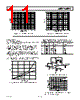
13 / 16 page  REV. B AD8057/AD8058 –13– For 0 V input, the outputs of the op amps want to be at 2.5 V, which is the midsupply level of the ADCs. This is accomplished by first taking the 2.5 V reference output of the ADC and divid- ing it by two by a pair of 1 k Ω resistors. The resulting 1.25 V is applied to each op amp’s positive input. This voltage is then multiplied by the gain of +2 of the op amps to provide a 2.5 V level at each output. The assumption for this circuit is that the input signal is bipolar with respect to ground and the circuit must be dc-coupled. This implies the existence of a negative supply elsewhere in the sys- tem. This circuit uses –5 V as the negative supply for the AD8058. If the AD8058 negative supply were tied to ground, there would be a problem at the input of the noninverting op amp. The input common-mode voltage can only go to within 1 V of the negative rail. Since this circuit requires that the positive inputs operate with a 1.25 V bias, there is not enough room to swing this voltage in the negative direction. The inverting stage does not have this problem because its common-mode input voltage remains fixed at 1.25 V. If dc coupling is not required, various ac coupling techniques can be used to eliminate this problem. Layout The AD8057 and AD8058 are high speed op amps and should be used in a board layout that follows standard high speed design rules. All the signal traces should be as short and direct as pos- sible. In particular, the parasitic capacitance on the inverting input of each device should be kept to a minimum to avoid excessive peaking and other undesirable performance. The power supplies should be bypassed very close to the power pins of the package with 0.1 µF in parallel with a larger, approxi- mately 10 µF tantalum capacitor. These capacitors should be connected to a ground plane that is either on an inner layer or fills the area of the board that is not used for other signals. |
|
|
リンク URL |
| ALLDATASHEETはお客様のビジネスに役立ちますか? [ DONATE ] |
Alldatasheetは | 広告 | お問い合わせ | プライバシーポリシー | データシートへのリンク | リンク交換 | メーカーリスト All Rights Reserved©Alldatasheet.com |
| Russian : Alldatasheetru.com | Korean : Alldatasheet.co.kr | Spanish : Alldatasheet.es | French : Alldatasheet.fr | Italian : Alldatasheetit.com Portuguese : Alldatasheetpt.com | Polish : Alldatasheet.pl | Vietnamese : Alldatasheet.vn Indian : Alldatasheet.in | Mexican : Alldatasheet.com.mx | British : Alldatasheet.co.uk | New Zealand : Alldatasheet.co.nz |
|
Family Site : ic2ic.com |
icmetro.com |
 Japanese ▼
 English
 Chinese
 German
 Japanese
 Russian
 Korean
 Spanish
 French
 Italian
 Portuguese
 Polish
 Vietnamese
 Indian
 Mexican
 British
 New Zealand