|
データシートサーチシステム |
|
|
データシートサーチシステム |
|
ST7SCR データシート(PDF) 9 Page - STMicroelectronics |
|
|
|||||||||||||||||||||||||||||
ST7SCR データシート(HTML) 9 Page - STMicroelectronics |
|
|
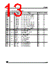
9 / 101 page  ST7SCR 9/101 Notes 1. Keyboard interface 2. It is mandatory to connect all available VDD and VDDA pins to the supply voltage and all VSS and VSSA pins to ground. 57 PA4 I/O CT XX X X Port A4 58 PA5 I/O CT XX X X Port A5 59 21 24 SELF2 O CT An External inductance must be connected to these pins for the step up converter (refer to Figure 5 to choose the right capacitance) 60 21 24 SELF1 O CT 61 22 1 DIODE S CT An External diode must be connected to this pin for the step up converter (refer to Figure 5 to choose the right component) 62 23 2 GNDA S Ground 63 24 3 GND S 64 1 4 CDRVCC O CT X Smartcard Supply pin Pin n° Pin Name Level Port / Control Main Function (after reset) Alternate Function Input Output |
|
リンク URL |
| ALLDATASHEETはお客様のビジネスに役立ちますか? [ DONATE ] |
Alldatasheetは | 広告 | お問い合わせ | プライバシーポリシー | データシートへのリンク | リンク交換 | メーカーリスト All Rights Reserved©Alldatasheet.com |
| Russian : Alldatasheetru.com | Korean : Alldatasheet.co.kr | Spanish : Alldatasheet.es | French : Alldatasheet.fr | Italian : Alldatasheetit.com Portuguese : Alldatasheetpt.com | Polish : Alldatasheet.pl | Vietnamese : Alldatasheet.vn Indian : Alldatasheet.in | Mexican : Alldatasheet.com.mx | British : Alldatasheet.co.uk | New Zealand : Alldatasheet.co.nz |
|
Family Site : ic2ic.com |
icmetro.com |
 Japanese ▼
 English
 Chinese
 German
 Japanese
 Russian
 Korean
 Spanish
 French
 Italian
 Portuguese
 Polish
 Vietnamese
 Indian
 Mexican
 British
 New Zealand