|
データシートサーチシステム |
|
|
データシートサーチシステム |
|
USBDF02W5 データシート(PDF) 5 Page - STMicroelectronics |
|
|
|||||||||||||||||||||||||||||
USBDF02W5 データシート(HTML) 5 Page - STMicroelectronics |
|
|
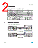
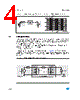
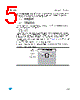
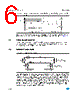
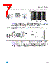
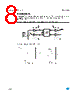
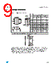
5 / 11 page  USBDFxxW5 Application information 5/11 To have a good approximation of the remaining voltages at both Vin and Vout stages, we give the typical dynamical resistance value Rd. Taking into account the following hypothesis: Rt > Rd, Rg > R and Rload > Rd, gives these formulas:: The results of the calculation done for VPP = 8 kV, Rg = 330 W (IEC61000-4-2 standard), VBR = 7 V (typ.) and Rd = 1 Ω (typ.) give: Vinput = 31.2 V Voutput = 7.95 V This confirms the very low remaining voltage across the device to be protected. It is also important to note that in this approximation the parasitic inductance effect was not taken into account. This could be few tenths of volts during few ns at the Vin side. This parasitic effect is not present at the Vout side due the low current involved after the resistance R. The measurements results shown below show very clearly (Figure 7.) the high efficiency of the ESD protection : ● no influence of the parasitic inductances on Vout stage ● output clamping voltage very close to VBR (positive strike) and -VF (negative strike) Figure 6. Measurement board V= input V= output R.V + R. V gBR d g R.V + R . V t BR d input Rg Rt TEST BOARD ESD SURGE 15 kV Air Discharge Vin Vout |
|
|
リンク URL |
| ALLDATASHEETはお客様のビジネスに役立ちますか? [ DONATE ] |
Alldatasheetは | 広告 | お問い合わせ | プライバシーポリシー | データシートへのリンク | リンク交換 | メーカーリスト All Rights Reserved©Alldatasheet.com |
| Russian : Alldatasheetru.com | Korean : Alldatasheet.co.kr | Spanish : Alldatasheet.es | French : Alldatasheet.fr | Italian : Alldatasheetit.com Portuguese : Alldatasheetpt.com | Polish : Alldatasheet.pl | Vietnamese : Alldatasheet.vn Indian : Alldatasheet.in | Mexican : Alldatasheet.com.mx | British : Alldatasheet.co.uk | New Zealand : Alldatasheet.co.nz |
|
Family Site : ic2ic.com |
icmetro.com |
 Japanese ▼
 English
 Chinese
 German
 Japanese
 Russian
 Korean
 Spanish
 French
 Italian
 Portuguese
 Polish
 Vietnamese
 Indian
 Mexican
 British
 New Zealand