|
データシートサーチシステム |
|
|
データシートサーチシステム |
|
H8SX1663 データシート(PDF) 1021 Page - Renesas Technology Corp |
|
|
|||||||||||||||||||||||||||||
H8SX1663 データシート(HTML) 1021 Page - Renesas Technology Corp |
|
|
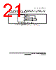
1021 / 1158 page  Section 22 Clock Pulse Generator Rev.1.00 Jun. 07, 2006 Page 969 of 1102 REJ09B0294-0100 Figure 22.11 shows the external circuitry recommended for the PLL circuit. Separate PLLVcc and PLLVss from the other Vcc and Vss lines at the board power supply source, and be sure to insert bypass capacitors CPB and CB close to the pins. PLLVCC PLLVSS VCC VSS Rp: 100 Ω CPB: 0.1 µF* CB: 0.1 µF* Note: * CB and CPB are laminated ceramic capacitors. Figure 22.11 Recommended External Circuitry for PLL Circuit |
|
リンク URL |
| ALLDATASHEETはお客様のビジネスに役立ちますか? [ DONATE ] |
Alldatasheetは | 広告 | お問い合わせ | プライバシーポリシー | データシートへのリンク | リンク交換 | メーカーリスト All Rights Reserved©Alldatasheet.com |
| Russian : Alldatasheetru.com | Korean : Alldatasheet.co.kr | Spanish : Alldatasheet.es | French : Alldatasheet.fr | Italian : Alldatasheetit.com Portuguese : Alldatasheetpt.com | Polish : Alldatasheet.pl | Vietnamese : Alldatasheet.vn Indian : Alldatasheet.in | Mexican : Alldatasheet.com.mx | British : Alldatasheet.co.uk | New Zealand : Alldatasheet.co.nz |
|
Family Site : ic2ic.com |
icmetro.com |
 Japanese ▼
 English
 Chinese
 German
 Japanese
 Russian
 Korean
 Spanish
 French
 Italian
 Portuguese
 Polish
 Vietnamese
 Indian
 Mexican
 British
 New Zealand