|
データシートサーチシステム |
|
|
データシートサーチシステム |
|
AD8278ARMZ-R7 データシート(PDF) 3 Page - Analog Devices |
|
|
|||||||||||||||||||||||||||||
AD8278ARMZ-R7 データシート(HTML) 3 Page - Analog Devices |
|
|
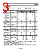
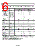
3 / 24 page  AD8278 Rev. 0 | Page 3 of 24 SPECIFICATIONS VS = ±5 V to ±15 V, VREF = 0 V, TA = 25°C, RL = 10 kΩ connected to ground, G = ½ difference amplifier configuration, unless otherwise noted. Table 2. Parameter Conditions G = ½ Unit Grade B Grade A Min Typ Max Min Typ Max INPUT CHARACTERISTICS System Offset1 50 100 50 250 μV vs. Temperature TA = −40°C to +85°C 100 250 μV Average Temperature Coefficient TA = −40°C to +85°C 0.3 1 2 5 μV/°C vs. Power Supply VS = ±5 V to ±18 V 2.5 5 μV/V Common-Mode Rejection Ratio (RTI) VS = ±15 V, VCM = ±27 V, RS = 0 Ω 80 74 dB Input Voltage Range2 −3(VS + 0.1) +3(VS − 1.5) −3(VS + 0.1) +3(VS − 1.5) V Impedance3 Differential 120 120 kΩ Common Mode 30 30 kΩ DYNAMIC PERFORMANCE Bandwidth 1 1 MHz Slew Rate 1.1 1.4 1.1 1.4 V/μs Settling Time to 0.01% 10 V step on output, CL = 100 pF 9 9 μs Settling Time to 0.001% 10 10 μs GAIN Gain Error 0.005 0.02 0.01 0.05 % Gain Drift TA = −40°C to +85°C 1 5 ppm/°C Gain Nonlinearity VOUT = 20 V p-p 5 10 ppm OUTPUT CHARACTERISTICS Output Voltage Swing4 VS = ±15 V, RL = 10 kΩ TA = −40°C to +85°C −VS + 0.2 +VS − 0.2 −VS + 0.2 +VS − 0.2 V Short-Circuit Current Limit ±15 ±15 mA Capacitive Load Drive 200 200 pF NOISE5 Output Voltage Noise f = 0.1 Hz to 10 Hz 1.4 1.4 μV p-p f = 1 kHz 47 50 47 50 nV/√Hz POWER SUPPLY Supply Current6 200 200 μA vs. Temperature TA = −40°C to +85°C 250 250 μA Operating Voltage Range7 ±2 ±18 ±2 ±18 V TEMPERATURE RANGE Operating Range −40 +125 −40 +125 °C 1 Includes input bias and offset current errors, RTO (referred to output) 2 The input voltage range may also be limited by absolute maximum input voltage or by the output swing. See the Input Voltage Range section in the Theory of Operation for details. 3 Internal resistors are trimmed to be ratio matched and have ±20% absolute accuracy. 4 Output voltage swing varies with supply voltage and temperature. See Figure 20 through Figure 23 for details. 5 Includes amplifier voltage and current noise, as well as noise from internal resistors. 6 Supply current varies with supply voltage and temperature. See Figure 24 and Figure 26 for details. 7 Unbalanced dual supplies can be used, such as −VS = −0.5 V and +VS = +2 V. The positive supply rail must be at least 2 V above the negative supply and reference voltage. |
|
|
リンク URL |
| ALLDATASHEETはお客様のビジネスに役立ちますか? [ DONATE ] |
Alldatasheetは | 広告 | お問い合わせ | プライバシーポリシー | データシートへのリンク | リンク交換 | メーカーリスト All Rights Reserved©Alldatasheet.com |
| Russian : Alldatasheetru.com | Korean : Alldatasheet.co.kr | Spanish : Alldatasheet.es | French : Alldatasheet.fr | Italian : Alldatasheetit.com Portuguese : Alldatasheetpt.com | Polish : Alldatasheet.pl | Vietnamese : Alldatasheet.vn Indian : Alldatasheet.in | Mexican : Alldatasheet.com.mx | British : Alldatasheet.co.uk | New Zealand : Alldatasheet.co.nz |
|
Family Site : ic2ic.com |
icmetro.com |
 Japanese ▼
 English
 Chinese
 German
 Japanese
 Russian
 Korean
 Spanish
 French
 Italian
 Portuguese
 Polish
 Vietnamese
 Indian
 Mexican
 British
 New Zealand