2-4
RF2103P
Rev B1 010720
2
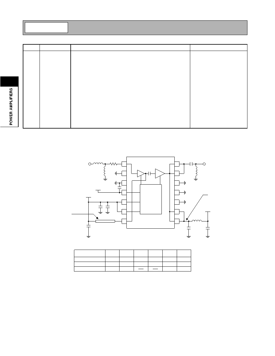
Application Schematic
Pin
Function
Description
Interface Schematic
14
RF OUT
Amplifier RF output. This is an unmatched collector output of the final
amplifier transistor. It is internally connected to pins 8, 9, 13 and 14 to
provide low series inductance and flexibility in output matching. Bias for
the final power amplifier output transistor must also be provided
through two of these four pins. Typically, pins 8 and 9 are connected to
a network that provides the DC bias and also creates a second har-
monic trap. For 915MHz operation, this harmonic trap network is simply
a single 2pF capacitor from both pins to ground. This capacitor series
resonates with internal bond wires at two times the operating fre-
quency, effectively shorting out the second harmonic. Shorting out this
harmonic serves to increase the amplifier’s maximum output power and
efficiency, as well as to lower the level of the second harmonic output.
Typically, pins 13 and 14 are externally connected very close to the
package and used as the RF output with a matching network that pre-
sents the optimum load impedance to the PA for maximum power and
efficiency, as well as providing DC blocking at the output. Shunt protec-
tion diodes are included to clip peak voltage excursions above approxi-
mately 15V to prevent voltage breakdown in worst case conditions.
1
2
3
4
5
6
7
14
13
12
11
10
9
8
BIAS
CIRCUITS
PRE AMP
FPA
100 pF
100
pF
C2
C1
330 pF
1
µF
L1
L2
V
CC
RF OUT
22
Ω
12 nH
6.8 nH
V
B
V
CC
100 pF
.01" x .2"
(PCB material: FR-4,
Thickness:0.031")
RF IN
For lower frequency
operation: Cut trace
on board and insert
inductor L4
FREQUENCY (MHz) L1 (nH)
L3 (nH)
L2 (nH)
L4 (nH)
C1 (pF)
C2 (pF)
275
480
915
20
15
10
20
20
10
12
6.8
4.7
18
12
6.8
6.8
3.3
4
2
For lower frequency
operation: Cut trace
on board and insert
inductor L3

 Japanese ▼
 English
 Chinese
 German
 Japanese
 Russian
 Korean
 Spanish
 French
 Italian
 Portuguese
 Polish
 Vietnamese
 Indian
 Mexican
 British
 New Zealand


