|
データシートサーチシステム |
|
|
データシートサーチシステム |
|
AD623ARZ-R7 データシート(PDF) 15 Page - Analog Devices |
|
|
|||||||||||||||||||||||||||||
AD623ARZ-R7 データシート(HTML) 15 Page - Analog Devices |
|
|
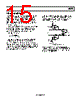
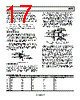
15 / 24 page  AD623 Rev. D | Page 15 of 24 THEORY OF OPERATION The AD623 is an instrumentation amplifier based on a modified classic 3-op-amp approach, to assure single or dual supply operation even at common-mode voltages at the negative supply rail. Low voltage offsets, input and output, as well as absolute gain accuracy, and one external resistor to set the gain, make the AD623 one of the most versatile instrumentation amplifiers in its class. The input signal is applied to PNP transistors acting as voltage buffers and providing a common-mode signal to the input amplifiers (see Figure 41). An absolute value 50 kΩ resistor in each amplifier feedback assures gain programmability. The differential output is C G O V R V ⎟⎟ ⎠ ⎞ ⎜⎜ ⎝ ⎛ + = kΩ 100 1 The differential voltage is then converted to a single-ended voltage using the output amplifier, which also rejects any common-mode signal at the output of the input amplifiers. Because the amplifiers can swing to either supply rail, as well as have their common-mode range extended to below the negative supply rail, the range over which the AD623 can operate is further enhanced (see Figure 20 and Figure 21). The output voltage at Pin 6 is measured with respect to the potential at Pin 5. The impedance of the reference pin is 100 kΩ; therefore, in applications requiring V/I conversion, a small resistor between Pin 5 and Pin 6 is all that is needed. POSITIVE SUPPLY 7 4 INVERTING 2 7 4 NEGATIVE SUPPLY NONINVERTING 3 50kΩ 50kΩ 50kΩ 50kΩ 50kΩ 50kΩ OTUPUT 6 REF 5 8 1 GAIN Figure 41. Simplified Schematic Note that the bandwidth of the in-amp decreases as gain is increased. This occurs because the internal op-amps are the standard voltage feedback design. At unity gain, the output amplifier limits the bandwidth. |
|
|
リンク URL |
| ALLDATASHEETはお客様のビジネスに役立ちますか? [ DONATE ] |
Alldatasheetは | 広告 | お問い合わせ | プライバシーポリシー | データシートへのリンク | リンク交換 | メーカーリスト All Rights Reserved©Alldatasheet.com |
| Russian : Alldatasheetru.com | Korean : Alldatasheet.co.kr | Spanish : Alldatasheet.es | French : Alldatasheet.fr | Italian : Alldatasheetit.com Portuguese : Alldatasheetpt.com | Polish : Alldatasheet.pl | Vietnamese : Alldatasheet.vn Indian : Alldatasheet.in | Mexican : Alldatasheet.com.mx | British : Alldatasheet.co.uk | New Zealand : Alldatasheet.co.nz |
|
Family Site : ic2ic.com |
icmetro.com |
 Japanese ▼
 English
 Chinese
 German
 Japanese
 Russian
 Korean
 Spanish
 French
 Italian
 Portuguese
 Polish
 Vietnamese
 Indian
 Mexican
 British
 New Zealand