|
データシートサーチシステム |
|
|
データシートサーチシステム |
|
ADA4077-2ARMZ-R7 データシート(PDF) 18 Page - Analog Devices |
|
|
|||||||||||||||||||||||||||||
ADA4077-2ARMZ-R7 データシート(HTML) 18 Page - Analog Devices |
|
|
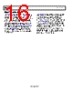
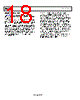
18 / 20 page  ADA4077-2 Data Sheet Rev. 0 | Page 18 of 20 PROPER BOARD LAYOUT The ADA4077-2 is a high precision device. To ensure optimum performance at the PCB level, care must be taken in the design of the board layout. To avoid leakage currents, maintain a clean and moisture-free board surface. Coating the surface creates a barrier to moisture accumulation and helps reduce parasitic resistance on the board. Keeping supply traces short and properly bypassing the power supplies minimizes power supply disturbances caused by output current variation, such as when driving an ac signal into a heavy load. Connect bypass capacitors as closely as possible to the device supply pins. Stray capacitances are a concern at the outputs and the inputs of the amplifier. It is recommended that signal traces be kept at least 5 mm from supply lines to minimize coupling. A variation in temperature across the PCB can cause a mismatch in the Seebeck voltages at solder joints and other points where dissimilar metals are in contact, resulting in thermal voltage errors. To minimize these thermocouple effects, orient resistors so heat sources warm both ends equally. Input signal paths should contain matching numbers and types of components, where possible, to match the number and type of thermocouple junctions. For example, dummy components such as zero value resistors can be used to match real resistors in the opposite input path. Place matching components in close proximity to each other and orient them in the same manner. Ensure that leads are of equal length so that thermal conduction is in equilibrium. Keep heat sources on the PCB as far away from amplifier input circuitry as is practical. The use of a ground plane is highly recommended. A ground plane reduces EMI noise and helps to maintain a constant temperature across the circuit board. |
|
|
リンク URL |
| ALLDATASHEETはお客様のビジネスに役立ちますか? [ DONATE ] |
Alldatasheetは | 広告 | お問い合わせ | プライバシーポリシー | データシートへのリンク | リンク交換 | メーカーリスト All Rights Reserved©Alldatasheet.com |
| Russian : Alldatasheetru.com | Korean : Alldatasheet.co.kr | Spanish : Alldatasheet.es | French : Alldatasheet.fr | Italian : Alldatasheetit.com Portuguese : Alldatasheetpt.com | Polish : Alldatasheet.pl | Vietnamese : Alldatasheet.vn Indian : Alldatasheet.in | Mexican : Alldatasheet.com.mx | British : Alldatasheet.co.uk | New Zealand : Alldatasheet.co.nz |
|
Family Site : ic2ic.com |
icmetro.com |
 Japanese ▼
 English
 Chinese
 German
 Japanese
 Russian
 Korean
 Spanish
 French
 Italian
 Portuguese
 Polish
 Vietnamese
 Indian
 Mexican
 British
 New Zealand