|
データシートサーチシステム |
|
|
データシートサーチシステム |
|
PCDC1008-R215EMO データシート(PDF) 46 Page - International Rectifier |
|
|
|||||||||||||||||||||||||||||
PCDC1008-R215EMO データシート(HTML) 46 Page - International Rectifier |
|
|
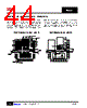
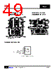
46 / 51 page  IR3447 46 www.irf.com © 2013 International Rectifier July 17, 2013 SOLDER RESIST IR recommends that the larger Power or Land Area pads are Solder Mask Defined (SMD). This allows the underlying Copper traces to be as large as possible, which helps in terms of current carrying capability and device cooling capability. When using SMD pads, the underlying copper traces should be at least 0.05mm larger (on each edge) than the Solder Mask window, in order to accommodate any layer to layer misalignment. (i.e. 0.1mm in X & Y). However, for the smaller Signal type leads around the edge of the device, IR recommends that these are Non Solder Mask Defined or Copper Defined. When using NSMD pads, the Solder Resist Window should be larger than the Copper Pad by at least 0.025mm on each edge, (i.e. 0.05mm in X & Y), in order to accommodate any layer to layer misalignment. Ensure that the solder resist in-between the smaller signal lead areas are at least 0.15mm wide, due to the high x/y aspect ratio of the solder mask strip. SOLDER MASK DESIGN PAD SIZES (DETAIL 1) SOLDER MASK DESIGN PAD SIZES (DETAIL 2) |
|
リンク URL |
| ALLDATASHEETはお客様のビジネスに役立ちますか? [ DONATE ] |
Alldatasheetは | 広告 | お問い合わせ | プライバシーポリシー | データシートへのリンク | リンク交換 | メーカーリスト All Rights Reserved©Alldatasheet.com |
| Russian : Alldatasheetru.com | Korean : Alldatasheet.co.kr | Spanish : Alldatasheet.es | French : Alldatasheet.fr | Italian : Alldatasheetit.com Portuguese : Alldatasheetpt.com | Polish : Alldatasheet.pl | Vietnamese : Alldatasheet.vn Indian : Alldatasheet.in | Mexican : Alldatasheet.com.mx | British : Alldatasheet.co.uk | New Zealand : Alldatasheet.co.nz |
|
Family Site : ic2ic.com |
icmetro.com |
 Japanese ▼
 English
 Chinese
 German
 Japanese
 Russian
 Korean
 Spanish
 French
 Italian
 Portuguese
 Polish
 Vietnamese
 Indian
 Mexican
 British
 New Zealand