|
データシートサーチシステム |
|
|
データシートサーチシステム |
|
AD7871JP データシート(PDF) 5 Page - Analog Devices |
|
|
|||||||||||||||||||||||||||||
AD7871JP データシート(HTML) 5 Page - Analog Devices |
|
|
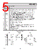
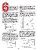
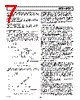
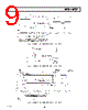
5 / 16 page  AD7871/AD7872 –5– REV. D AD7872 PIN FUNCTION DESCRIPTION DIP No. Mnemonic Function 1 CONTROL Control Input. With this pin at 0 V, the SCLK is noncontinuous; with this pin at –5 V, the SCLK is continuous. 2 CONVST Convert Start. A low to high transition on this input puts the track/hold into the hold mode. This input is asynchronous to the CLK. 3 CLK Clock Input. An external TTL-compatible clock may be applied to this input. Alternatively, tying this pin to VSS, enables the internal laser-trimmed oscillator. 4 SSTRB This is an active low three-state output that provides a framing pulse for serial data. An external 4.7 k Ω pull-up resistor is required on SSTRB. 5 SCLK Serial Clock. SCLK is the gated serial clock output derived from the internal or external ADC clock. If the 14/ 8/CLK input is at –5 V, then the SCLK runs continuously. With CONTROL at 0 V, it is gated off (three-state) after serial transmission is complete. SCLK is an open-drain output and requires an external 2 k Ω pull-up resistor. 6 SDATA Serial Data. This is the three-state serial data output used in conjunction with SCLK and SSTRB in serial data transmission. Serial data is valid on the falling edge of SCLK, when SSTRB is low. An external 4.7 k Ω pull-up resistor is required on SDATA. 7 NC No Connect. 8 DGND Digital Ground. Ground return for digital circuitry. 9VDD Positive Supply for analog circuitry, +5 V ± 5%. 10 NC No Connect. 11 CREF Decoupling point for on-chip reference. Connect 10 nF capacitor between this pin and AGND. 12 AGND Analog Ground. Ground reference for analog circuitry. 13 REF OUT Voltage Reference Output. The internal 3 V reference is provided at this pin. The external load capability is 500 µA. 14 VIN Analog Input. The input range is ±3 V. 15 VSS Negative Supply, –5 V ± 5%. 16 VDD Positive Supply for analog circuitry, +5 V ± 5%. Pin 16 and Pin 9 should be connected together. PIN CONFIGURATIONS DIP DIP, SOIC PLCC |
|
|
リンク URL |
| ALLDATASHEETはお客様のビジネスに役立ちますか? [ DONATE ] |
Alldatasheetは | 広告 | お問い合わせ | プライバシーポリシー | データシートへのリンク | リンク交換 | メーカーリスト All Rights Reserved©Alldatasheet.com |
| Russian : Alldatasheetru.com | Korean : Alldatasheet.co.kr | Spanish : Alldatasheet.es | French : Alldatasheet.fr | Italian : Alldatasheetit.com Portuguese : Alldatasheetpt.com | Polish : Alldatasheet.pl | Vietnamese : Alldatasheet.vn Indian : Alldatasheet.in | Mexican : Alldatasheet.com.mx | British : Alldatasheet.co.uk | New Zealand : Alldatasheet.co.nz |
|
Family Site : ic2ic.com |
icmetro.com |
 Japanese ▼
 English
 Chinese
 German
 Japanese
 Russian
 Korean
 Spanish
 French
 Italian
 Portuguese
 Polish
 Vietnamese
 Indian
 Mexican
 British
 New Zealand