|
データシートサーチシステム |
|
|
データシートサーチシステム |
|
AS1331 データシート(PDF) 11 Page - ams AG |
|
|
|||||||||||||||||||||||||||||
AS1331 データシート(HTML) 11 Page - ams AG |
|
|
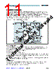
11 / 17 page  www.austriamicrosystems.com/DC-DC_Buck-Boost/AS1331 Revision 1.04 10 - 16 AS1331 Datasheet - D e t a i l e d D e s c r i p t i o n 8 Detailed Description The synchronous buck-boost converter AS1331 uses a Power Save Mode control technique to reach a high efficiency over a wide dynamic range of load currents. The output voltage is monitored by a comparator with 3% accuracy. The Power Save Mode puts the device into “sleep mode” when VOUT is above its programmed reference threshold. Meaning, the switching is stopped and only quiescent current is drawn from the power source. The switching is started again when VOUT drops below the reference threshold and the output capacitor is charged again. The numbers of current pulses which are necessary to load the output capacitor are set by the value of the output capacitor, the load current, and the comparator hysteresis (~1%). Figure 23. AS1331 - Block Diagram - Fixed Output Voltage Modes of Operation When VOUT drops below the reference threshold, the AS1331 switches on the transistors SW A and SW C until the inductor current reaches approximately 400mA. In the next step SW A and SW D are closed and depending on the difference between VIN and VOUT the inductor current raises, falls or stays constant. VIN > VOUT: The inductor current is going up to 600mA. VIN ~ VOUT: The device stops after 2µs. VIN < VOUT: The inductor current falls down to 0mA. If the inductor current is not 0mA, the transistors SW B and SW D are closed to ramp down the current to zero. If VOUT is still below the threshold voltage the next cycle is started. If IMAX (600mA) wasn’t reached in the previous cycle, SW A and SW D are closed until the inductor current is 600mA. Note: The 4-switch-mode (SW A+SW C => SW B+SW D => SW A + SW C...) and also the buck-mode (SW A+SW D => SW B+SW D => SW A+SW D...) are never used. Start-Up Mode At start-up the switch SW D is disabled and its diode is used to transfer current to the output capacitor until VOUT reaches approximately 2.15V. The inductor current is controlled by an alternate algorithm during start-up. Note: Do not apply loads >1mA until VOUT = 2.3V is reached. VIN SW1 SW2 SW A SW B SW C SW D VIN VIN 1.6V 600mA VOUT PGND GND EN Peak Current Limit UVLO State Machine and Logic VBEST Gate Drivers and Anticross Conduction IZERO Detect 1.25V Thermal Shutdown Shutdown VOUT VBEST R1 R2 FB VOUT Comp AS1331 |
|
|
リンク URL |
| ALLDATASHEETはお客様のビジネスに役立ちますか? [ DONATE ] |
Alldatasheetは | 広告 | お問い合わせ | プライバシーポリシー | データシートへのリンク | リンク交換 | メーカーリスト All Rights Reserved©Alldatasheet.com |
| Russian : Alldatasheetru.com | Korean : Alldatasheet.co.kr | Spanish : Alldatasheet.es | French : Alldatasheet.fr | Italian : Alldatasheetit.com Portuguese : Alldatasheetpt.com | Polish : Alldatasheet.pl | Vietnamese : Alldatasheet.vn Indian : Alldatasheet.in | Mexican : Alldatasheet.com.mx | British : Alldatasheet.co.uk | New Zealand : Alldatasheet.co.nz |
|
Family Site : ic2ic.com |
icmetro.com |
 Japanese ▼
 English
 Chinese
 German
 Japanese
 Russian
 Korean
 Spanish
 French
 Italian
 Portuguese
 Polish
 Vietnamese
 Indian
 Mexican
 British
 New Zealand