|
データシートサーチシステム |
|
|
データシートサーチシステム |
|
AD587 データシート(PDF) 7 Page - Analog Devices |
|
|
|||||||||||||||||||||||||||||
AD587 データシート(HTML) 7 Page - Analog Devices |
|
|
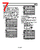
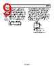
7 / 12 page  AD587 Rev. H | Page 7 of 12 TURN-ON TIME Upon application of power (cold start), the time required for the output voltage to reach its final value within a specified error band is defined as the turn-on settling time. Two compo- nents normally associated with this are the time for the active circuits to settle and the time for the thermal gradients on the chip to stabilize. Figure 7, Figure 8, and Figure 9 show the turn- on characteristics of the AD587. These figures show the settling to be about 60 μs to 0.01%. Note the absence of any thermal tails when the horizontal scale is expanded to 1 ms/cm in Figure 8. Output turn-on time is modified when an external noise reduc- tion capacitor is used. When present, this capacitor acts as an additional load to the current source of the internal Zener diode, resulting in a somewhat longer turn-on time. In the case of a 1 μF capacitor, the initial turn-on time is approximately 400 ms to 0.01%, as shown in Figure 9. 100 10 0% 10V 1mV 90 +VIN VOUT 20µs Figure 7. Electrical Turn-On 100 90 10 0% 10V 1ms 20V +VIN VOUT Figure 8. Extended Time Scale 100 90 10 0% 1V 100ms 10V +VIN VOUT Figure 9. Turn-On with 1 μF CN DYNAMIC PERFORMANCE The output buffer amplifier is designed to provide the AD587 with static and dynamic load regulation that is superior to less complete references. Many ADCs and DACs present transient current loads to the reference, and poor reference response can degrade the con- verter’s performance. Figure 11 and Figure 12 display the characteristics of the AD587 output amplifier driving a 0 mA to 10 mA load. AD587 VOUT 7.0V 1kΩ 10V 0V VL Figure 10. Transient Load Test Circuit 100 90 10 0% 50mV 1µs 10V VL VOUT Figure 11. Large-Scale Transient Response |
|
|
リンク URL |
| ALLDATASHEETはお客様のビジネスに役立ちますか? [ DONATE ] |
Alldatasheetは | 広告 | お問い合わせ | プライバシーポリシー | データシートへのリンク | リンク交換 | メーカーリスト All Rights Reserved©Alldatasheet.com |
| Russian : Alldatasheetru.com | Korean : Alldatasheet.co.kr | Spanish : Alldatasheet.es | French : Alldatasheet.fr | Italian : Alldatasheetit.com Portuguese : Alldatasheetpt.com | Polish : Alldatasheet.pl | Vietnamese : Alldatasheet.vn Indian : Alldatasheet.in | Mexican : Alldatasheet.com.mx | British : Alldatasheet.co.uk | New Zealand : Alldatasheet.co.nz |
|
Family Site : ic2ic.com |
icmetro.com |
 Japanese ▼
 English
 Chinese
 German
 Japanese
 Russian
 Korean
 Spanish
 French
 Italian
 Portuguese
 Polish
 Vietnamese
 Indian
 Mexican
 British
 New Zealand