|
データシートサーチシステム |
|
|
データシートサーチシステム |
|
AD688 データシート(PDF) 12 Page - Analog Devices |
|
|
|||||||||||||||||||||||||||||
AD688 データシート(HTML) 12 Page - Analog Devices |
|
|
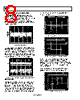
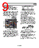
12 / 16 page  AD688 Rev. B | Page 12 of 16 10V 0V VL 1k Ω 10V VOUT 10V A4 A3 + – + – Figure 27. Load Crosstalk Test Circuit 100 90 10 0% 1mV 5V 2 µs VOUT VL Figure 28. Load Crosstalk Attempts to drive a large capacitive load (in excess of 1000 pF) may result in ringing or oscillation, as shown in the step response photo (Figure 29). This is due to the additional pole formed by the load capacitance and the output impedance of the amplifier, which consumes phase margin. The recom- mended method of driving capacitive loads of this magnitude is shown in Figure 30. The 150 Ω resistor isolates the capacitive load from the output stage, while the 10 kΩ resistor provides a dc feedback path and preserves the output accuracy. The 1 µF capacitor provides a high frequency feedback loop. The performance of this circuit is shown in Figure 31. 100 90 10 0% 10V 1V 200 µs VIN VOUT Figure 29. Output Amplifier Step Response, CL = 1 µF VIN VOUT + – 10k Ω 1 µF CL 1 µF 150 Ω Figure 30. Compensation for Capacitive Loads 100 90 10 0% 10V 1V 200 µs VIN VOUT Figure 31. Output Amplifier Step Response Using Figure 30 Compensation BRIDGE DRIVER CIRCUIT The Wheatstone bridge is a common transducer. In its simplest form, a bridge consists of four 2-terminal elements connected to form a quadrilateral, a source of excitation connected along one of the diagonals and a detector comprising the other diagonal. In this unipolar drive configuration, the output voltage of the bridge is riding on a common-mode voltage signal equal to approximately VIN/2. Further processing of this signal may necessarily be limited to high common-mode rejection techniques such as instrumentation or isolation amplifiers. However, if the bridge is driven from a pair of bipolar supplies, then the common-mode voltage is ideally eliminated and the restrictions on any processing elements that follow are relaxed. As shown in Figure 32, the AD688 is an excellent choice for the control element in a bipolar bridge driver scheme. Transistors Q1 and Q2 serve as series pass elements to boost the current drive capability to the 57 mA required by the typical 350 Ω bridge. A differential gain stage may still be required if the bridge balance is not perfect. R3 RB R1 R2 R4 R5 R6 –VS +VS A1 A4 AD688 A3 A2 Q1 = 2N3904 220 Ω +15V –15V 220 Ω Q2 = 2N3906 EO + – 7 6 4 3 14 2 15 16 5 9 10 8 12 11 13 1 Figure 32. Bipolar Bridge Drive |
|
|
リンク URL |
| ALLDATASHEETはお客様のビジネスに役立ちますか? [ DONATE ] |
Alldatasheetは | 広告 | お問い合わせ | プライバシーポリシー | データシートへのリンク | リンク交換 | メーカーリスト All Rights Reserved©Alldatasheet.com |
| Russian : Alldatasheetru.com | Korean : Alldatasheet.co.kr | Spanish : Alldatasheet.es | French : Alldatasheet.fr | Italian : Alldatasheetit.com Portuguese : Alldatasheetpt.com | Polish : Alldatasheet.pl | Vietnamese : Alldatasheet.vn Indian : Alldatasheet.in | Mexican : Alldatasheet.com.mx | British : Alldatasheet.co.uk | New Zealand : Alldatasheet.co.nz |
|
Family Site : ic2ic.com |
icmetro.com |
 Japanese ▼
 English
 Chinese
 German
 Japanese
 Russian
 Korean
 Spanish
 French
 Italian
 Portuguese
 Polish
 Vietnamese
 Indian
 Mexican
 British
 New Zealand