|
データシートサーチシステム |
|
|
データシートサーチシステム |
|
LT1371 データシート(PDF) 11 Page - Linear Technology |
|
|
|||||||||||||||||||||||||||||
LT1371 データシート(HTML) 11 Page - Linear Technology |
|
|
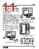
11 / 16 page  11 LT1371 APPLICATIO S I FOR ATIO maximum output load current and will also be increased if poor quality (high ESR) output capacitors are used. The addition of a 0.0047 µF capacitor on the VC pin reduces switching frequency ripple to only a few millivolts. A low value for RC will also reduce VC pin ripple, but loop phase margin may be inadequate. Layout Considerations For maximum efficiency, LT1371 switch rise and fall times are made as short as possible. To prevent radiation and high frequency resonance problems, proper layout of the components connected to the switch node is essential. B field (magnetic) radiation is minimized by keeping output diode, Switch pin and output bypass capacitor leads as short as possible. Figures 3, 4 and 5 show recommended positions for these components. E field radiation is kept low by minimizing the length and area of all traces con- nected to the Switch pin. A ground plane should always be used under the switcher circuitry to prevent interplane coupling. The high speed switching current path is shown schemati- cally in Figure 6. Minimum lead length in this path is essential to ensure clean switching and low EMI. The path including the switch, output diode and output capacitor is the only one containing nanosecond rise and fall times. Keep this path as short as possible. VIN S/S GND FB VSW VC NFB CONNECT GROUND PIN AND TAB DIRECTLY TO GROUND PLANE C D KEEP PATH FROM VSW, OUTPUT DIODE, OUTPUT CAPACITORS AND GROUND RETURN AS SHORT AS POSSIBLE C LT1371 • F03 Figure 3. Layout Considerations— R Package VIN S/S GND FB VSW VC NFB CONNECT GROUND PIN AND TAB DIRECTLY TO GROUND PLANE. TAB MAY BE SOLDERED OR BOLTED TO GROUND PLANE* C D KEEP PATH FROM VSW, OUTPUT DIODE, OUTPUT CAPACITORS AND GROUND RETURN AS SHORT AS POSSIBLE *SEE T7 PACKAGE LAYOUT CONSIDERATIONS FOR VERTICAL MOUNTING OF THE T7 PACKAGE C LT1371 • F04 Figure 4. Layout Considerations— T7 Package Figure 6 LOAD VOUT L1 SWITCH NODE LT1371 • F06 VIN HIGH FREQUENCY CIRCULATING PATH D CONNECT ALL GROUND PINS TO GROUND PLANE C C KEEP PATH FROM VSW, OUTPUT DIODE, OUTPUT CAPACITORS AND GROUND RETURN AS SHORT AS POSSIBLE LT1371 • F05 VSW NC VSW GND GND GND GND NC NC GND VC FB NFB GND GND GND GND SHDN SYNC VIN Figure 5. Layout Considerations— SW Package |
|
|
リンク URL |
| ALLDATASHEETはお客様のビジネスに役立ちますか? [ DONATE ] |
Alldatasheetは | 広告 | お問い合わせ | プライバシーポリシー | データシートへのリンク | リンク交換 | メーカーリスト All Rights Reserved©Alldatasheet.com |
| Russian : Alldatasheetru.com | Korean : Alldatasheet.co.kr | Spanish : Alldatasheet.es | French : Alldatasheet.fr | Italian : Alldatasheetit.com Portuguese : Alldatasheetpt.com | Polish : Alldatasheet.pl | Vietnamese : Alldatasheet.vn Indian : Alldatasheet.in | Mexican : Alldatasheet.com.mx | British : Alldatasheet.co.uk | New Zealand : Alldatasheet.co.nz |
|
Family Site : ic2ic.com |
icmetro.com |
 Japanese ▼
 English
 Chinese
 German
 Japanese
 Russian
 Korean
 Spanish
 French
 Italian
 Portuguese
 Polish
 Vietnamese
 Indian
 Mexican
 British
 New Zealand