|
データシートサーチシステム |
|
|
データシートサーチシステム |
|
LT1959 データシート(PDF) 12 Page - Linear Technology |
|
|
|||||||||||||||||||||||||||||
LT1959 データシート(HTML) 12 Page - Linear Technology |
|
|
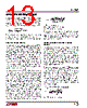
12 / 24 page  12 LT1959 APPLICATIONS INFORMATION Ceramic Capacitors Higher value, lower cost ceramic capacitors are now available in smaller case sizes. These are ideal for input bypassing because of their high ripple rating and tolerance to turn-on surges. As output capacitors, caution must be used. Solid tantalum capacitor’s ESR generates a loop “zero” at 5kHz to 50kHz that is beneficial in giving accept- able loop phase margin. Ceramic capacitors remain ca- pacitive to beyond 300kHz and usually resonate with their ESL before ESR becomes effective. When using ceramic output capacitors, the loop compensation pole frequency must be reduced by a typical factor of 10. OUTPUT RIPPLE VOLTAGE Figure 3 shows a typical output ripple voltage waveform for the LT1959. Ripple voltage is determined by the high frequency impedance of the output capacitor, and ripple current through the inductor. Peak-to-peak ripple current through the inductor into the output capacitor is: I VV V VL f P OUT IN OUT IN -P = () − () ()( )( ) For high frequency switchers, the sum of ripple current slew rates may also be relevant and can be calculated from: Σ dI dt V L IN = Peak-to-peak output ripple voltage is the sum of a triwave created by peak-to-peak ripple current times ESR, and a square wave created by parasitic inductance (ESL) and ripple current slew rate. Capacitive reactance is assumed to be small compared to ESR or ESL. V I ESR ESL dI dt RIPPLE = ()( )+() P-P Σ Example: with VIN =10V, VOUT = 5V, L = 10µH, ESR = 0.1Ω, ESL = 10nH: IA dI dt VA mV RIPPLE P-P P-P = () − () () = == = ()( )+ =+ = − − − 510 5 10 10 10 500 10 05 10 10 10 10 05 01 10 10 10 0 05 0 01 60 63 6 6 96 •• . • .. • .. Σ VOUT AT IOUT = 1A VOUT AT IOUT = 50mA INDUCTOR CURRENT AT IOUT = 1A 0.5 µs/DIV 1374 F03 INDUCTOR CURRENT AT IOUT = 50mA 20mV/DIV 0.5A/DIV Figure 3. LT1959 Ripple Voltage Waveform CATCH DIODE The suggested catch diode (D1) is a 1N5821 Schottky, or its Motorola equivalent, MBR330. It is rated at 3A average forward current and 30V reverse voltage. Typical forward voltage is 0.5V at 3A. The diode conducts current only during switch off time. Peak reverse voltage is equal to regulator input voltage. Average forward current in normal operation can be calculated from: I IV V V D AVG OUT IN OUT IN ( )= − () This formula will not yield values higher than 3A with maximum load current of 4.25A unless the ratio of input to output voltage exceeds 3.4:1. The only reason to consider a larger diode is the worst-case condition of a high input voltage and overloaded (not shorted) output. Under short- circuit conditions, foldback current limit will reduce diode current to less than 2.6A, but if the output is overloaded |
|
|
リンク URL |
| ALLDATASHEETはお客様のビジネスに役立ちますか? [ DONATE ] |
Alldatasheetは | 広告 | お問い合わせ | プライバシーポリシー | データシートへのリンク | リンク交換 | メーカーリスト All Rights Reserved©Alldatasheet.com |
| Russian : Alldatasheetru.com | Korean : Alldatasheet.co.kr | Spanish : Alldatasheet.es | French : Alldatasheet.fr | Italian : Alldatasheetit.com Portuguese : Alldatasheetpt.com | Polish : Alldatasheet.pl | Vietnamese : Alldatasheet.vn Indian : Alldatasheet.in | Mexican : Alldatasheet.com.mx | British : Alldatasheet.co.uk | New Zealand : Alldatasheet.co.nz |
|
Family Site : ic2ic.com |
icmetro.com |
 Japanese ▼
 English
 Chinese
 German
 Japanese
 Russian
 Korean
 Spanish
 French
 Italian
 Portuguese
 Polish
 Vietnamese
 Indian
 Mexican
 British
 New Zealand