|
データシートサーチシステム |
|
|
データシートサーチシステム |
|
TS19310ACX6RFG データシート(PDF) 5 Page - Taiwan Semiconductor Company, Ltd |
|
|
|||||||||||||||||||||||||||||
TS19310ACX6RFG データシート(HTML) 5 Page - Taiwan Semiconductor Company, Ltd |
|
|
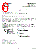
5 / 8 page  TS19310A/B Single-Stage PFC TRIAC Dimmable LED Driver 5/8 Version: A14 Typical Application Circuit Application Information Function Description The TS19310 is boundary conduction mode (BCM) operation with constant on time based regulator design to achieve high power factor performance. The TS19310 has built-in functions of phase dimmable, and included protection function related VCC over-voltage protection, open-LED protection, short-LED protection, over- temperature protection, primary side current limit, and gate clamp is within. The TS19310 is the sense switch current from CS voltage multiplier by test data input signal (TDIS) to get the output current information by system close loop feedback. The average output current can express by below formula. S S P OUT R 2 * 0.333 N N I Where: ● I OUT is the average output current ● N P is the primary-side turn ratio ● N S is the secondary-side turn ratio ● 0.333 is the reference potential setting of IC ● 2 is the reference potential setting of IC ● η is the efficiency ● R S is the sensing resistor connected between the MOSFET source and the GND Pin Detail Pin 1: Compensation This is the output of the gm amplifier. Connect with a suitable RC network to ground. Pin 2: Ground GND is the reference node of internal circuit. |
|
|
リンク URL |
| ALLDATASHEETはお客様のビジネスに役立ちますか? [ DONATE ] |
Alldatasheetは | 広告 | お問い合わせ | プライバシーポリシー | データシートへのリンク | リンク交換 | メーカーリスト All Rights Reserved©Alldatasheet.com |
| Russian : Alldatasheetru.com | Korean : Alldatasheet.co.kr | Spanish : Alldatasheet.es | French : Alldatasheet.fr | Italian : Alldatasheetit.com Portuguese : Alldatasheetpt.com | Polish : Alldatasheet.pl | Vietnamese : Alldatasheet.vn Indian : Alldatasheet.in | Mexican : Alldatasheet.com.mx | British : Alldatasheet.co.uk | New Zealand : Alldatasheet.co.nz |
|
Family Site : ic2ic.com |
icmetro.com |
 Japanese ▼
 English
 Chinese
 German
 Japanese
 Russian
 Korean
 Spanish
 French
 Italian
 Portuguese
 Polish
 Vietnamese
 Indian
 Mexican
 British
 New Zealand