|
データシートサーチシステム |
|
|
データシートサーチシステム |
|
PAM8303CBSC データシート(PDF) 12 Page - Diodes Incorporated |
|
|
|||||||||||||||||||||||||||||
PAM8303CBSC データシート(HTML) 12 Page - Diodes Incorporated |
|
|
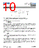
12 / 17 page  PAM8303C Document number: DSxxxxx Rev. 1 - 2 12 of 17 www.diodes.com June 2013 © Diodes Incorporated PAM8303C A Product Line of Diodes Incorporated Application Information (cont.) PCB Layout Guidelines Grounding It is recommended to use plain grounding or separate grounds. Do not use one line connecting power GND and analog GND. Noise currents in the output power stage need to be returned to output noise ground and nowhere else. When these currents circulate elsewhere, they may get into the power supply, or the signal ground, etc, even worse, they may form a loop and radiate noise. Any of these instances results in degraded amplifier performance. The output noise ground that the logical returns for the output noise currents associated with Class-D switching must tie to system ground at the power exclusively. Signal currents for the inputs, reference need to be returned to quite ground. This ground only ties to the signal components and the GND pin. GND then ties to system ground. Power Supply Line As same to the ground, VDD and PVDD need to be separately connected to the system power supply. It is recommended that all the trace could be routed as short and thick as possible. For the power line layout, just imagine water stream, any barricade placed in the trace (shown in Figure 2) could result in the bad performance of the amplifier. Figure 2. Power Line Components Placement Decoupling capacitors-As previously described, the high-frequency 1µF decoupling capacitors should be placed as close to the power supply terminals (VDD and PVDD) as possible. Large bulk power supply decoupling capacitors (10µF or greater) should be placed near the PAM8303C on the PVDD terminal. Input resistors and capacitors need to be placed very close to input pins. Output filter - The ferrite EMI filter should be placed as close to the output terminals as possible for the best EMI performance, and the capacitors used in the filters should be grounded to system ground. |
|
|
リンク URL |
| ALLDATASHEETはお客様のビジネスに役立ちますか? [ DONATE ] |
Alldatasheetは | 広告 | お問い合わせ | プライバシーポリシー | データシートへのリンク | リンク交換 | メーカーリスト All Rights Reserved©Alldatasheet.com |
| Russian : Alldatasheetru.com | Korean : Alldatasheet.co.kr | Spanish : Alldatasheet.es | French : Alldatasheet.fr | Italian : Alldatasheetit.com Portuguese : Alldatasheetpt.com | Polish : Alldatasheet.pl | Vietnamese : Alldatasheet.vn Indian : Alldatasheet.in | Mexican : Alldatasheet.com.mx | British : Alldatasheet.co.uk | New Zealand : Alldatasheet.co.nz |
|
Family Site : ic2ic.com |
icmetro.com |
 Japanese ▼
 English
 Chinese
 German
 Japanese
 Russian
 Korean
 Spanish
 French
 Italian
 Portuguese
 Polish
 Vietnamese
 Indian
 Mexican
 British
 New Zealand