|
データシートサーチシステム |
|
|
データシートサーチシステム |
|
MIC4685 データシート(PDF) 2 Page - Micrel Semiconductor |
|
|
|||||||||||||||||||||||||||||
MIC4685 データシート(HTML) 2 Page - Micrel Semiconductor |
|
|
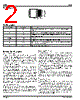
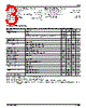
2 / 15 page  MIC4685 Micrel MIC4685 2 September 2002 Pin Description Pin Number Pin Name Pin Function 1 BS Bootstrap Voltage Node (External Component): Connect to external boost capacitor. 2 IN Supply (Input): Unregulated +4V to 30V supply voltage (34V transient) 3 FB Feedback (Input): Outback voltage feedback to regulator. Connect to 1.235V tap of resistive divider. 4, Tab GND Ground 5 EN Enable (Input): Logic high = enable; logic low = shutdown 6 SW Switch (Output): Emitter of NPN output switch. Connect to external storage inductor and Schottky diode. 7 NC No Connect. Tie this pin to ground. Pin Configuration 7NC 6SW 5EN 4 GND 3FB 2IN 1BS SPAK-07L (R) Detailed Pin Description Switch (SW, Pin 6) The switch pin is tied to the emitter of the main internal NPN transistor. This pin is biased up to the input voltage minus the V SAT of the main NPN pass element. The emitter is also driven negative when the output inductor’s magnetic field collapses at turn-off. During the OFF time the SW pin is clamped by the output Schottky diode to a –0.5V typically. Ground (GND, Pin 4, Tab) There are two main areas of concern when it comes to the ground pin, EMI and ground current. In a buck regulator or any other non-isolated switching regulator the output capacitor(s) and diode(s) ground is referenced back to the switching regulator’s or controller’s ground pin. Any resis- tance between these reference points causes an offset voltage/IR drop proportional to load current and poor load regulation. This is why its important to keep the output grounds placed as close as possible to the switching regulator’s ground pin. To keep radiated EMI to a minimum it is neces- sary to place the input capacitor ground lead as close as possible to the switching regulator’s ground pin. Input Voltage (V IN, Pin 2) The V IN pin is the collector of the main NPN pass element. This pin is also connected to the internal regulator. The output diode or clamping diode should have its cathode as close as possible to this point to avoid voltage spikes adding to the voltage across the collector. Bootstrap (BS, Pin 1) The bootstrap pin in conjunction with the external bootstrap capacitor provides a bias voltage higher than the input voltage to the MIC4685’s main NPN pass element. The bootstrap capacitor sees the dv/dt of the switching action at the SW pin as an AC voltage. The bootstrap capacitor then couples the AC voltage back to the BS pin plus the dc offset of V IN where it is rectified and used to provide additional drive to the main switch, in this case a NPN transistor. This additional drive reduces the NPN’s saturation voltage and increases efficiency, from a V SAT of 1.8V, and 75% efficiency to a V SAT of 0.5V and 88% efficiency respectively. Feedback (FB, Pin 3) The feedback pin is tied to the inverting side of an error amplifier. The noninverting side is tied to a 1.235V bandgap reference. An external resistor voltage divider is required from the output to ground, with the center tied to the feedback pin. Enable (EN, Pin 5) The enable (EN) input is used to turn on the regulator and is TTL compatible. Note: connect the enable pin to the input if unused. A logic-high enables the regulator. A logic-low shuts down the regulator and reduces the stand-by quiescent input current to typically 150 µA. The enable pin has an upper threshold of 2.0V minimum and lower threshold of 0.8V maximum. The hysterisis provided by the upper and lower thresholds acts as an UVLO and prevents unwanted turn on of the regulator due to noise. |
|
|
リンク URL |
| ALLDATASHEETはお客様のビジネスに役立ちますか? [ DONATE ] |
Alldatasheetは | 広告 | お問い合わせ | プライバシーポリシー | データシートへのリンク | リンク交換 | メーカーリスト All Rights Reserved©Alldatasheet.com |
| Russian : Alldatasheetru.com | Korean : Alldatasheet.co.kr | Spanish : Alldatasheet.es | French : Alldatasheet.fr | Italian : Alldatasheetit.com Portuguese : Alldatasheetpt.com | Polish : Alldatasheet.pl | Vietnamese : Alldatasheet.vn Indian : Alldatasheet.in | Mexican : Alldatasheet.com.mx | British : Alldatasheet.co.uk | New Zealand : Alldatasheet.co.nz |
|
Family Site : ic2ic.com |
icmetro.com |
 Japanese ▼
 English
 Chinese
 German
 Japanese
 Russian
 Korean
 Spanish
 French
 Italian
 Portuguese
 Polish
 Vietnamese
 Indian
 Mexican
 British
 New Zealand