|
データシートサーチシステム |
|
|
データシートサーチシステム |
|
AD8067ART-R2 データシート(PDF) 19 Page - Analog Devices |
|
|
|||||||||||||||||||||||||||||
AD8067ART-R2 データシート(HTML) 19 Page - Analog Devices |
|
|
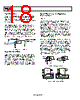
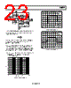
19 / 24 page  AD8067 Rev. 0 | Page 19 of 24 GROUNDING To minimize parasitic inductances and ground loops in high speed, densely populated boards, a ground plane layer is critical. Understanding where the current flows in a circuit is critical in the implementation of high speed circuit design. The length of the current path is directly proportional to the magnitude of the parasitic inductances and thus the high frequency impedance of the path. Fast current changes in an inductive ground return will create unwanted noise and ringing. The length of the high frequency bypass capacitor leads is critical. A parasitic inductance in the bypass grounding will work against the low impedance created by the bypass capacitor. Because load currents flow from supplies as well as ground, the load should be placed at the same physical location as the bypass capacitor ground. For large values of capacitors, which are intended to be effective at lower frequencies, the current return path length is less critical. POWER SUPPLY BYPASSING Power supply pins are actually inputs and care must be taken to provide a clean, low noise dc voltage source to these inputs. The bypass capacitors have two functions: 1. Provide a low impedance path for unwanted frequencies from the supply inputs to ground, thereby reducing the effect of noise on the supply lines 2. Provide localized charge storage—this is usually accomplished with larger electrolytic capacitors Decoupling methods are designed to minimize the bypassing impedance at all frequencies. This can be accomplished with a combination of capacitors in parallel to ground. Good quality ceramic chip capacitors (X7R or NPO) should be used and always kept as close to the amplifier package as possible. A parallel combination of a 0.1 µF ceramic and a 10 µF electrolytic, covers a wide range of rejection for unwanted noise. The 10 µF capacitor is less critical for high frequency bypassing, and in most cases, one per supply line is sufficient. |
|
|
リンク URL |
| ALLDATASHEETはお客様のビジネスに役立ちますか? [ DONATE ] |
Alldatasheetは | 広告 | お問い合わせ | プライバシーポリシー | データシートへのリンク | リンク交換 | メーカーリスト All Rights Reserved©Alldatasheet.com |
| Russian : Alldatasheetru.com | Korean : Alldatasheet.co.kr | Spanish : Alldatasheet.es | French : Alldatasheet.fr | Italian : Alldatasheetit.com Portuguese : Alldatasheetpt.com | Polish : Alldatasheet.pl | Vietnamese : Alldatasheet.vn Indian : Alldatasheet.in | Mexican : Alldatasheet.com.mx | British : Alldatasheet.co.uk | New Zealand : Alldatasheet.co.nz |
|
Family Site : ic2ic.com |
icmetro.com |
 Japanese ▼
 English
 Chinese
 German
 Japanese
 Russian
 Korean
 Spanish
 French
 Italian
 Portuguese
 Polish
 Vietnamese
 Indian
 Mexican
 British
 New Zealand