 |
データシートサーチシステム |
|
|
データシートサーチシステム |
|
The question interval is too short.
Please try again in a few seconds.

Hello, Please ask a question about AP3003S-3.3E1 Datasheet
# Example questions:
➢ What is the approximate efficiency of the 5.0v version of this converter when the input voltage is 20v and the load current is 3a?
➢ The datasheet presents data for multiple versions (5.0v, 12v, adjustable). how does the load regulation (figure 10) appear to differ between the 5.0v and 12v versions?
➢ What is the typical switch saturation voltage when the switch current is 2a, assuming a junction temperature of 25°c?
| Part No. | AP3003S-3.3E1 |
| Manufacturer | BCDSEMI |
| Size | 258 Kbytes |
| Pages | 16 pages |
| Description | 150kHz 3A BUCK DC-DC CONVERTER |

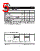
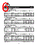
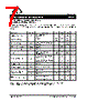
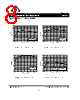


Device Summary: (Assuming this is a Switching Regulator/Power Supply Controller)
1. General
️· Type: Likely a switching regulator or power supply controller (details on specific type are missing)
️· Manufacturer: BCD Semiconductor Manufacturing Limited
️· Documentation Revision: Rev. 1.0/1.1 (two different revisions exist for different figures.)
2. Electrical Characteristics (Based on the best available data)
️· Input Voltage Range: While not explicitly stated, figures suggest a range of approximately 0-36V (likely nominal 12V in many tests)
️· Output Voltage: The figures mention 5.0V. The document also notes this is configurable.
️· Switching Frequency: Not directly mentioned, but implied by figures related to switching.
️· Quiescent Current (Iq):
- Varies with Junction Temperature (TJ). At TJ=25°C, Iq seems to be approximately 180mA.
- Also varies with Input Voltage, shown in Figure 15 (Shutdown Quiescent Current vs. Input Voltage).
️· Switch Current Limit: Figure 12. Approximately 10A at a junction temperature of around 25°C. This limit decreases as junction temperature increases.
️· Switch Saturation Voltage: Figure 11. Appears to be around 3.5V.
️· Efficiency: Not explicitly stated, but figures showing input voltage vs. efficiency imply reasonable efficiency for a wide range of operating conditions.
3. Transient Response (Based on limited data)
️· Load Regulation: Figure 13. Shows a load regulation of approximately +/-0.1V (100mV) during a test using a supply voltage of 12V.
️· Line Regulation: Figure 14. Shows a line regulation of approximately +/- 0.05V during a test using a supply voltage of 12V.
4. Protection/Limits
️· Switch Current Limit: A current limit exists to protect the switch, approximately 10A. The value changes with junction temperature.
️· Junction Temperature (TJ): A critical operating parameter for performance and protection. Refer to specific figures for limits under various conditions.
️· Shutdown Quiescent Current: Appears to be minimal when in shutdown mode.
Important Notes and Caveats:
️· Missing Information: The provided text represents *snippets* from a datasheet. Crucial details are absent:
- Specific regulator topology (e.g., buck, boost, buck-boost)
- Detailed input/output capacitor requirements.
- Control loop compensation details.
- Minimum load requirements.
- Detailed startup behavior.
️· Figure Dependence: Values are often dependent on the specific figure being referenced (e.g., TJ, Vin, Vout, Load).
️· Incomplete Test Conditions: Test conditions (temperature, load, input voltage, etc.) are not always clearly defined for every figure.
️· Documentation Revision: The two versions of documentation present different figures. Use figures corresponding to the revision you're working with.
️· This is not a complete datasheet. This summary should *not* be used as a substitute for the full documentation. The full datasheet is absolutely critical before using this device in a design.
Device Summary: (Assuming this is a Switching Regulator/Power Supply Controller)
1. General
️· Type: Likely a switching regulator or power supply controller (details on specific type are missing)
️· Manufacturer: BCD Semiconductor Manufacturing Limited
️· Documentation Revision: Rev. 1.0/1.1 (two different revisions exist for different figures.)
2. Electrical Characteristics (Based on the best available data)
️· Input Voltage Range: While not explicitly stated, figures suggest a range of approximately 0-36V (likely nominal 12V in many tests)
️· Output Voltage: The figures mention 5.0V. The document also notes this is configurable.
️· Switching Frequency: Not directly mentioned, but implied by figures related to switching.
️· Quiescent Current (Iq):
- Varies with Junction Temperature (TJ). At TJ=25°C, Iq seems to be approximately 180mA.
- Also varies with Input Voltage, shown in Figure 15 (Shutdown Quiescent Current vs. Input Voltage).
️· Switch Current Limit: Figure 12. Approximately 10A at a junction temperature of around 25°C. This limit decreases as junction temperature increases.
️· Switch Saturation Voltage: Figure 11. Appears to be around 3.5V.
️· Efficiency: Not explicitly stated, but figures showing input voltage vs. efficiency imply reasonable efficiency for a wide range of operating conditions.
3. Transient Response (Based on limited data)
️· Load Regulation: Figure 13. Shows a load regulation of approximately +/-0.1V (100mV) during a test using a supply voltage of 12V.
️· Line Regulation: Figure 14. Shows a line regulation of approximately +/- 0.05V during a test using a supply voltage of 12V.
4. Protection/Limits
️· Switch Current Limit: A current limit exists to protect the switch, approximately 10A. The value changes with junction temperature.
️· Junction Temperature (TJ): A critical operating parameter for performance and protection. Refer to specific figures for limits under various conditions.
️· Shutdown Quiescent Current: Appears to be minimal when in shutdown mode.
Important Notes and Caveats:
️· Missing Information: The provided text represents *snippets* from a datasheet. Crucial details are absent:
- Specific regulator topology (e.g., buck, boost, buck-boost)
- Detailed input/output capacitor requirements.
- Control loop compensation details.
- Minimum load requirements.
- Detailed startup behavior.
️· Figure Dependence: Values are often dependent on the specific figure being referenced (e.g., TJ, Vin, Vout, Load).
️· Incomplete Test Conditions: Test conditions (temperature, load, input voltage, etc.) are not always clearly defined for every figure.
️· Documentation Revision: The two versions of documentation present different figures. Use figures corresponding to the revision you're working with.
️· This is not a complete datasheet. This summary should *not* be used as a substitute for the full documentation. The full datasheet is absolutely critical before using this device in a design.
| Part No. | AP3003S-3.3E1 |
| Manufacturer | BCDSEMI |
| Size | 258 Kbytes |
| Pages | 16 pages |
| Description | 150kHz 3A BUCK DC-DC CONVERTER |
| ALLDATASHEETはお客様のビジネスに役立ちますか? [ DONATE ] |
Alldatasheetは | 広告 | お問い合わせ | プライバシーポリシー | データシートへのリンク | リンク交換 | メーカーリスト All Rights Reserved©Alldatasheet.com |
| Russian : Alldatasheetru.com | Korean : Alldatasheet.co.kr | Spanish : Alldatasheet.es | French : Alldatasheet.fr | Italian : Alldatasheetit.com Portuguese : Alldatasheetpt.com | Polish : Alldatasheet.pl | Vietnamese : Alldatasheet.vn Indian : Alldatasheet.in | Mexican : Alldatasheet.com.mx | British : Alldatasheet.co.uk | New Zealand : Alldatasheet.co.nz |
|
Family Site : ic2ic.com |
icmetro.com |
 Japanese ▼
  English
 Chinese
 German
 Russian
 Korean
 Spanish
 French
 Italian
 Portuguese
 Polish
 Vietnamese
 Indian
 Mexican
 British
 New Zealand