 |
データシートサーチシステム |
|
|
データシートサーチシステム |
|
The question interval is too short.
Please try again in a few seconds.

Hello, Please ask a question about FM25V02 Datasheet
# Example questions:
➢ Describe the function of the /hold pin and explain the timing constraints that must be met when using it to pause and resume a serial operation.
➢ Explain how the block protect bits (bp0 and bp1) function and how they interact with the wpen bit and the /w pin to provide write protection for different sections of memory.
➢ What are the key differences between a standard read operation and a fast read operation on the fm25v02, and when might you choose one over the other?
| Part No. | FM25V02 |
| Manufacturer | CYPRESS |
| Size | 549 Kbytes |
| Pages | 17 pages |
| Description | 256Kb Serial 3V F-RAM Memory |


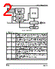


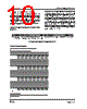


1. General Overview & Key Features
️· What it is: The FM25V02 is a 256kb SPI FRAM (Ferroelectric RAM) device. FRAM combines the speed of RAM with the non-volatility of Flash memory.
️· Fast Writes: Enables fast write speeds, avoiding the need for page buffers common in Serial Flash.
️· Low Power: Includes a Sleep Mode for reduced power consumption.
️· Compatibility: Designed to be compatible with Serial Flash devices, including support for the FAST READ operation.
2. Pin Functions & Signals
️· /S (Serial Clock): The primary clock signal for all operations.
️· C (Serial Data Input): Used for sending commands and data to the device.
️· D (Serial Data Output): Used for receiving data from the device.
️· /HOLD: Can be used to interrupt serial operations without aborting them. Must be toggled while `/S` is low.
️· Q (Data Output): The data output pin.
3. Operating Modes & Commands
️· Read: Uses the `READ` OpCode followed by a two-byte address.
️· Write: Requires a `WREN` (Write Enable) OpCode, followed by a `WRITE` OpCode, then a two-byte address, then the data to be written. Data is written MSB first.
️· Fast Read: Similar to Read, but includes a dummy byte for latency. Uses the `FAST READ` OpCode, followed by a two-byte address and then a dummy byte.
️· Sleep Mode: Enters low power mode using the `SLEEP` OpCode. The device monitors `/S`. The device returns to normal operation on the next falling edge of `/S`.
️· Device ID Read (RDID): Uses the `RDID` OpCode to read Manufacturer ID and Product ID.
4. Memory Organization & Addressing
️· Memory Size: 256kb
️· Addressing: Uses 16-bit addresses (A14-A0).
️· Address Rollover: When the maximum address (7FFFh) is reached, the counter rolls over to 0000h.
5. Write Protection
️· WREN: Requires Write Enable before writing.
️· WPEN (Write Protection Enable): Controlled by the Status Register, allows to ignore the `/W` signal.
️· Block Protection (BP0, BP1): Enable write protection for different memory blocks. Block protection table shown in the document.
6. Sleep Mode Details
️· Entry: Uses the SLEEP OpCode (B9h).
️· Wakeup: Requires a falling edge of /S to return to normal operation (t REC, 400 μs max).
7. Device Identification (RDID)
️· Function: Allows to read manufacturer ID and product ID.
️· Opcode: RDID (9Fh).
1. General Overview & Key Features
️· What it is: The FM25V02 is a 256kb SPI FRAM (Ferroelectric RAM) device. FRAM combines the speed of RAM with the non-volatility of Flash memory.
️· Fast Writes: Enables fast write speeds, avoiding the need for page buffers common in Serial Flash.
️· Low Power: Includes a Sleep Mode for reduced power consumption.
️· Compatibility: Designed to be compatible with Serial Flash devices, including support for the FAST READ operation.
2. Pin Functions & Signals
️· /S (Serial Clock): The primary clock signal for all operations.
️· C (Serial Data Input): Used for sending commands and data to the device.
️· D (Serial Data Output): Used for receiving data from the device.
️· /HOLD: Can be used to interrupt serial operations without aborting them. Must be toggled while `/S` is low.
️· Q (Data Output): The data output pin.
3. Operating Modes & Commands
️· Read: Uses the `READ` OpCode followed by a two-byte address.
️· Write: Requires a `WREN` (Write Enable) OpCode, followed by a `WRITE` OpCode, then a two-byte address, then the data to be written. Data is written MSB first.
️· Fast Read: Similar to Read, but includes a dummy byte for latency. Uses the `FAST READ` OpCode, followed by a two-byte address and then a dummy byte.
️· Sleep Mode: Enters low power mode using the `SLEEP` OpCode. The device monitors `/S`. The device returns to normal operation on the next falling edge of `/S`.
️· Device ID Read (RDID): Uses the `RDID` OpCode to read Manufacturer ID and Product ID.
4. Memory Organization & Addressing
️· Memory Size: 256kb
️· Addressing: Uses 16-bit addresses (A14-A0).
️· Address Rollover: When the maximum address (7FFFh) is reached, the counter rolls over to 0000h.
5. Write Protection
️· WREN: Requires Write Enable before writing.
️· WPEN (Write Protection Enable): Controlled by the Status Register, allows to ignore the `/W` signal.
️· Block Protection (BP0, BP1): Enable write protection for different memory blocks. Block protection table shown in the document.
6. Sleep Mode Details
️· Entry: Uses the SLEEP OpCode (B9h).
️· Wakeup: Requires a falling edge of /S to return to normal operation (t REC, 400 μs max).
7. Device Identification (RDID)
️· Function: Allows to read manufacturer ID and product ID.
️· Opcode: RDID (9Fh).
| Part No. | FM25V02 |
| Manufacturer | CYPRESS |
| Size | 549 Kbytes |
| Pages | 17 pages |
| Description | 256Kb Serial 3V F-RAM Memory |
| ALLDATASHEETはお客様のビジネスに役立ちますか? [ DONATE ] |
Alldatasheetは | 広告 | お問い合わせ | プライバシーポリシー | データシートへのリンク | リンク交換 | メーカーリスト All Rights Reserved©Alldatasheet.com |
| Russian : Alldatasheetru.com | Korean : Alldatasheet.co.kr | Spanish : Alldatasheet.es | French : Alldatasheet.fr | Italian : Alldatasheetit.com Portuguese : Alldatasheetpt.com | Polish : Alldatasheet.pl | Vietnamese : Alldatasheet.vn Indian : Alldatasheet.in | Mexican : Alldatasheet.com.mx | British : Alldatasheet.co.uk | New Zealand : Alldatasheet.co.nz |
|
Family Site : ic2ic.com |
icmetro.com |
 Japanese ▼
  English
 Chinese
 German
 Russian
 Korean
 Spanish
 French
 Italian
 Portuguese
 Polish
 Vietnamese
 Indian
 Mexican
 British
 New Zealand