|
データシートサーチシステム |
|
|
データシートサーチシステム |
|
AD8450ASTZ データシート(PDF) 26 Page - Analog Devices |
|
|
|||||||||||||||||||||||||||||
AD8450ASTZ データシート(HTML) 26 Page - Analog Devices |
|
|
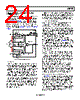
26 / 42 page  Data Sheet AD8450 Rev. B | Page 25 of 41 The unity-gain amplifier (VINT buffer) buffers the VINT pin and drives the VCTRL pin. The VCTRL pin is the control output of the AD8450 and the control input of the power converter. The VISET and VVSET voltage sources set the target constant current and the target constant voltage, respectively. When the CC and CV feedback loops are in steady state, the charging current is set at IBAT_SS = S IA ISET R G V × where: GIA is the PGIA gain. RS is the value of the shunt resistor. The target voltage is set at VBAT_SS = DA VSET G V where GDA is the PGDA gain. Because the offset voltage of the loop amplifiers is in series with the target voltage sources, VISET and VVSET, the high precision of these amplifiers minimizes this source of error. Figure 54 shows a typical CC/CV charging profile for a Li-Ion battery. In the first stage of the charging process, the battery is charged with a constant current (CC) of 1 A. When the battery voltage reaches a target voltage of 4.2 V, the charging process transitions such that the battery is charged with a constant voltage (CV) of 4.2 V. 1.25 0 0.25 0.50 0.75 1.00 5 0 1 2 3 4 0 5 4 3 2 1 TIME (Hours) CC CHARGE BEGINS TRANSITION FROM CC TO CV CC CHARGE ENDS Figure 54. Representative Constant Current to Constant Voltage Transition Near the End of a Battery Charging Cycle The following steps describe how the AD8450 implements the CC/CV charging profile (see Figure 53). In this scenario, the battery begins in the fully discharged state, and the system has just been turned on such that IBAT = 0 A at Time 0. 1. Because the voltages at the ISMEA and BVMEA pins are below the target voltages (VISET and VVSET) at Time 0, both integrators begin to ramp, increasing the voltage at the VINT node. 2. As the voltage at the VINT node increases, the voltage at the VCRTL node rises, and the output current of the power converter, IBAT, increases (assuming that an increasing voltage at the VCRTL node increases the output current of the power converter). 3. When the IBAT current reaches the CC steady state value, IBAT_SS, the battery voltage is still below the target steady state value, VBAT_SS. Therefore, the CV loop tries to keep pulling the VINT node up while the CC loop tries to keep it at its current voltage. At this point, the voltage at the ISMEA pin equals VISET, so the CC loop stops integrating. 4. Because the loop amplifiers can only pull the VINT node down due to the analog NOR circuit, the CC loop takes control of the charging feedback loop and the CV loop is disabled. 5. As the charging process continues, the battery voltage increases until it reaches the steady state value, VBAT_SS, and the voltage at the BVMEA pin reaches the target voltage, VVSET. 6. The CV loop tries to pull the VINT node down to reduce the charging current (IBAT) and prevent the battery voltage from rising any farther. At the same time, the CC loop tries to keep the VINT node at its current voltage to keep the battery current at IBAT_SS. 7. Because the loop amplifiers can only pull the VINT node down due to the analog NOR circuit, the CV loop takes control of the charging feedback loop and the CC loop is disabled. The analog NOR (minimum output selector) circuit that couples the outputs of the loop amplifiers is optimized to minimize the transition time from CC to CV control. Any delay in the trans- ition causes the CC loop to remain in control of the charge feedback loop after the battery voltage reaches its target value. Therefore, the battery voltage continues to rise beyond VBAT_SS until the control loop transitions; that is, the battery voltage overshoots its target voltage. When the CV loop takes control of the charge feedback loop, it reduces the battery voltage to the target voltage. A large overshoot in the battery voltage due to transition delays can damage the battery; thus, it is crucial to minimize delays by implementing a fast CC to CV transition. |
|
リンク URL |
| ALLDATASHEETはお客様のビジネスに役立ちますか? [ DONATE ] |
Alldatasheetは | 広告 | お問い合わせ | プライバシーポリシー | データシートへのリンク | リンク交換 | メーカーリスト All Rights Reserved©Alldatasheet.com |
| Russian : Alldatasheetru.com | Korean : Alldatasheet.co.kr | Spanish : Alldatasheet.es | French : Alldatasheet.fr | Italian : Alldatasheetit.com Portuguese : Alldatasheetpt.com | Polish : Alldatasheet.pl | Vietnamese : Alldatasheet.vn Indian : Alldatasheet.in | Mexican : Alldatasheet.com.mx | British : Alldatasheet.co.uk | New Zealand : Alldatasheet.co.nz |
|
Family Site : ic2ic.com |
icmetro.com |
 Japanese ▼
 English
 Chinese
 German
 Japanese
 Russian
 Korean
 Spanish
 French
 Italian
 Portuguese
 Polish
 Vietnamese
 Indian
 Mexican
 British
 New Zealand