|
データシートサーチシステム |
|
|
データシートサーチシステム |
|
AD7450ABRT-R2 データシート(PDF) 17 Page - Analog Devices |
|
|
|||||||||||||||||||||||||||||
AD7450ABRT-R2 データシート(HTML) 17 Page - Analog Devices |
|
|
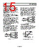
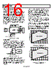
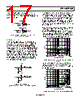
17 / 28 page  AD7440/AD7450A Rev. B | Page 17 of 28 Figure 30 shows examples of the inputs to VIN+ and VIN– for different values of VREF for VDD = 5 V. It also gives the maximum and minimum common-mode voltages for each reference value according to Figure 28. COMMON-MODE (CM) CMMIN = 1V CMMAX = 4V REFERENCE = 2V VIN– VIN+ 2V p-p COMMON-MODE (CM) CMMIN = 1.25V CMMAX = 3.75V REFERENCE = 2.5V VIN– VIN+ 2.5V p-p Figure 30. Examples of the Analog Inputs to VIN+ and VIN– for Different Values of VREF for VDD = 5 V Analog Input Structure Figure 31 shows the equivalent circuit of the analog input structure of the AD7440/AD7450A. The four diodes provide ESD protection for the analog inputs. Care must be taken to ensure that the analog input signals never exceed the supply rails by more than 300 mV. This causes these diodes to become forward biased and start conducting into the substrate. These diodes can conduct up to 10 mA without causing irreversible damage to the part. The capacitors, C1 in Figure 31, are typically 4 pF and can primarily be attributed to pin capacitance. The resistors are lumped components made up of the on resistance of the switches. The value of these resistors is typically about 100 Ω. The capacitors, C2, are the ADC’s sampling capacitors and have a capacitance of 16 pF typically. C1 C2 R1 D D C1 C2 R1 D D VDD VDD VIN+ VIN– Figure 31. Equivalent Analog Input Circuit Conversion Phase–Switches Open; Track Phase–Switches Closed For ac applications, removing high frequency components from the analog input signal through the use of an RC low-pass filter on the relevant analog input pins is recommended. In applica- tions where harmonic distortion and signal-to-noise ratio are critical, the analog input should be driven from a low impe- dance source. Large source impedances significantly affect the ac performance of the ADC. This may necessitate the use of an input buffer amplifier. The choice of op amp is a function of the particular application. When no amplifier is used to drive the analog input, the source impedance should be limited to low values. The maximum source impedance depends on the amount of total harmonic distortion (THD) that can be tolerated. The THD increases as the source impedance increases, and performance degrades. Figure 32 shows a graph of THD versus the analog input signal frequency for different source impedances for VDD = 5 V. 0 –100 –80 –60 –40 –20 10 100 1000 INPUT FREQUENCY (kHz) TA = 25°C VDD = 5V RIN = 1kΩ RIN = 510Ω RIN = 10Ω RIN = 300Ω Figure 32. THD vs. Analog Input Frequency for Various Source Impedances for VDD=5V Figure 33 shows a graph of the THD versus the analog input frequency for VDD of 5 V ± 5% and 3 V + 20%/–10%, while sampling at 1 MSPS with an SCLK of 18 MHz. In this case, the source impedance is 10 Ω. –50 –90 –85 –80 –75 –70 –65 –60 –55 10 100 1000 INPUT FREQUENCY (kHz) TA = 25°C VDD = 2.7V VDD = 3.6V VDD = 5.25V VDD = 4.75V Figure 33. THD vs. Analog Input Frequency for 3 V and 5 V Supply Voltages |
|
|
リンク URL |
| ALLDATASHEETはお客様のビジネスに役立ちますか? [ DONATE ] |
Alldatasheetは | 広告 | お問い合わせ | プライバシーポリシー | データシートへのリンク | リンク交換 | メーカーリスト All Rights Reserved©Alldatasheet.com |
| Russian : Alldatasheetru.com | Korean : Alldatasheet.co.kr | Spanish : Alldatasheet.es | French : Alldatasheet.fr | Italian : Alldatasheetit.com Portuguese : Alldatasheetpt.com | Polish : Alldatasheet.pl | Vietnamese : Alldatasheet.vn Indian : Alldatasheet.in | Mexican : Alldatasheet.com.mx | British : Alldatasheet.co.uk | New Zealand : Alldatasheet.co.nz |
|
Family Site : ic2ic.com |
icmetro.com |
 Japanese ▼
 English
 Chinese
 German
 Japanese
 Russian
 Korean
 Spanish
 French
 Italian
 Portuguese
 Polish
 Vietnamese
 Indian
 Mexican
 British
 New Zealand