|
データシートサーチシステム |
|
|
データシートサーチシステム |
|
LYT5216 データシート(PDF) 6 Page - Power Integrations, Inc. |
|
|
|||||||||||||||||||||||||||||
LYT5216 データシート(HTML) 6 Page - Power Integrations, Inc. |
|
|
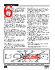
6 / 14 page  Rev. C 03/16 6 LYT5216-5228 www.power.com Figure 6. DER-515 PCB Layout Example using SO-16B D Package. Shows the Location of Critical Components and Loop Areas on the PCB Layout. To ensure that discontinuous conduction mode (DCM) operation of LYTSwitch-5 is maintained over line input and inductance tolerance variations, and to ensure for accurate output current regulation, it is recommended that the LYTSwitch-5 PIXls spreadsheet located at PI Expert web lab (http://piexpertweblab.power.com/site/login) should be used for magnetics calculations. EMI Considerations Total input capacitance affects PF and ATHD – increasing the value will degrade performance. With LYTSwitch-5, the combination of a low-side switching configuration and frequency jitter reduces EMI and enables the use of small and simple π (pi) filter. It also allows simple magnetic construction where the main winding can be wound continuously using the automated winding approach preferred for low-cost manufacturing. The recommended location of the EMI filter is after the bridge rectifier. This allows the use of regular film capacitors as opposed to more expensive safety rated X capacitors that would be required if the filter is placed before the bridge. Surge Immunity Consideration This design assumed a differential surge requirement of 3 kV which can be met easily with LYTSwitch-5 line overvoltage protection and using a RCD surge clamp circuit (D5, R2 and C3) and MOV (RV1). For lower differential surge requirement such as 1 kV, capacitor C3 can be reduced to 1 mF. Thermal and Lifetime Considerations Lighting applications present thermal challenges to the driver. In many cases the LED load dissipation determines the working ambient temperature experienced by the drive. Thermal evaluation should be performed with the driver inside the final enclosure. Temperature has a direct impact on driver and LED lifetime. For every 10 °C rise in temperature, component life is reduced by a factor of 2. Therefore it is important to verify and optimize the operating temperatures of all components. Quick Design Checklist Maximum Drain Voltage Verify that the peak drain voltage stress (VDS) does not exceed maximum acceptable drain voltage under all operating conditions, including start-up and fault conditions. Maximum Drain Current Measure the peak drain current under all operation conditions (including start-up and fault conditions). Look for transformer saturation (usually occurs at highest operating ambient tempera- tures). Verify that the peak current is less than the stated Absolute Maximum Rating in the data sheet. Thermal Check At maximum output power, for both minimum and maximum line voltage and maximum ambient temperature; verify that temperature specifications are not exceeded for the LYTSwitch-5, transformer, output diodes, output capacitors and clamp components. PCB Layout Considerations The EMI filter components should be located close together to improve filter effectiveness. Place the EMI filter components C1 and L1 as far away as possible from any switching nodes on the circuit board especially U1 drain node, output diode (D7) and the transformer (T1). Care should be taken in placing the components on the layout that are used for processing input signals for the feedback loop – any high frequency noise coupled to the signal pins of U1 may affect proper system operation. The critical components in DER-515 are R5, R9, C6, R4, R7 and R8. It is highly recommended that these components be placed very close to the pins of U1 (to minimize long traces which could serve as antenna) and far away as much as possible from any high voltage and high current nodes in the circuit board to avoid noise coupling. The bypass supply capacitor C5 should be placed directly across BYPASS pin and SOURCE pin of U1 for effective noise decoupling. As shown in Figure 6, minimize the loop areas of the following switching circuit elements to lessen the creation of EMI. • Loop area formed by the transformer output winding (T1), output rectifier diode (D7) and output capacitor (C8). • Loop area formed by transformer bias winding (T1), rectifier diode (D6) and filter capacitor (C7). • Loop area formed by input capacitor (C2), transformer (T1) main winding R10, C4 and internal MOSFET (U1). Lastly, unlike discrete MOSFET designs where heat sinking is through the drain tab and which generates significant EMI, the LYTSwitch-5 devices employ low-side switching and the ground potential SOURCE pins are used for heat sinking. This allows the designer to maximize the copper area for good thermal management but without having the risk of increased EMI. Design Tools Up-to-date information on design tools can be found at the Power Integrations web site: www.power.com LYTSwitch-5 PIXls spreadsheet is located at PI Expert web lab: http://piexpertweblab.power.com/site/login. FEEDBACK Pin Resistor R9 and C6 LINE SENSE Pin Resistor R4 Drain Current Sense R10 and C4 OUTPUT COMPENSATION Pin Resistor R5 BYPASS Pin Capacitor C5 Bias Diode Rectifier D6 and Filter C7 Output Capacitor TRF DRIVER CURRENT SENSE Pin Resistor R7 DATA OUTPUT Pin Resistor R8 Ouput Diode Rectifier D7 and Filter C8 PI-7795-120315 |
|
|
リンク URL |
| ALLDATASHEETはお客様のビジネスに役立ちますか? [ DONATE ] |
Alldatasheetは | 広告 | お問い合わせ | プライバシーポリシー | データシートへのリンク | リンク交換 | メーカーリスト All Rights Reserved©Alldatasheet.com |
| Russian : Alldatasheetru.com | Korean : Alldatasheet.co.kr | Spanish : Alldatasheet.es | French : Alldatasheet.fr | Italian : Alldatasheetit.com Portuguese : Alldatasheetpt.com | Polish : Alldatasheet.pl | Vietnamese : Alldatasheet.vn Indian : Alldatasheet.in | Mexican : Alldatasheet.com.mx | British : Alldatasheet.co.uk | New Zealand : Alldatasheet.co.nz |
|
Family Site : ic2ic.com |
icmetro.com |
 Japanese ▼
 English
 Chinese
 German
 Japanese
 Russian
 Korean
 Spanish
 French
 Italian
 Portuguese
 Polish
 Vietnamese
 Indian
 Mexican
 British
 New Zealand