|
データシートサーチシステム |
|
|
データシートサーチシステム |
|
AM29PDS322D データシート(PDF) 25 Page - SPANSION |
|
|
|||||||||||||||||||||||||||||
AM29PDS322D データシート(HTML) 25 Page - SPANSION |
|
|
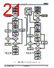
25 / 51 page  December 4, 2006 23569A5 Am29PDS322D 23 D A TA SH EET cycles, followed by a set-up command. Two additional unlock write cycles are then followed by the chip erase command, which in turn invokes the Embedded Erase algorithm. The device does not require the system to preprogram prior to erase. The Embedded Erase algo- rithm automatically preprograms and verifies the entire memory for an all zero data pattern prior to electrical erase. The system is not required to provide any con- trols or timings during these operations. Table 10 shows the address and data requirements for the chip erase command sequence. Start 555h/AAh 2AAh/55h XXXh/A0h 555h/20h Verify Byte? No Program Address/Program Data Data# Polling Device Last Address ? Programming Completed (BA) XXXh/90h XXXh/F0h Increment Address No Yes Yes Set Unlock Bypass Mode In Unlock Bypass Program Reset Unlock Bypass Mode Figure 4. Unlock Bypass Algorithm START Write Program Command Sequence Data Poll from System Verify Data? No Yes Last Address? No Yes Programming Completed Increment Address Embedded Program algorithm in progress Note: See Table 10 for program command sequence. Figure 5. Program Operation |
|
リンク URL |
| ALLDATASHEETはお客様のビジネスに役立ちますか? [ DONATE ] |
Alldatasheetは | 広告 | お問い合わせ | プライバシーポリシー | データシートへのリンク | リンク交換 | メーカーリスト All Rights Reserved©Alldatasheet.com |
| Russian : Alldatasheetru.com | Korean : Alldatasheet.co.kr | Spanish : Alldatasheet.es | French : Alldatasheet.fr | Italian : Alldatasheetit.com Portuguese : Alldatasheetpt.com | Polish : Alldatasheet.pl | Vietnamese : Alldatasheet.vn Indian : Alldatasheet.in | Mexican : Alldatasheet.com.mx | British : Alldatasheet.co.uk | New Zealand : Alldatasheet.co.nz |
|
Family Site : ic2ic.com |
icmetro.com |
 Japanese ▼
 English
 Chinese
 German
 Japanese
 Russian
 Korean
 Spanish
 French
 Italian
 Portuguese
 Polish
 Vietnamese
 Indian
 Mexican
 British
 New Zealand