|
データシートサーチシステム |
|
|
データシートサーチシステム |
|
STW81101ATR データシート(PDF) 20 Page - STMicroelectronics |
|
|
|||||||||||||||||||||||||||||
STW81101ATR データシート(HTML) 20 Page - STMicroelectronics |
|
|
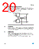
20 / 48 page  Circuit description STW81101 20/48 5.5 Phase frequency detector (PFD) The PFD takes inputs from the reference and the VCO dividers and produces an output proportional to the phase error. The PFD includes a delay gate that controls the width of the anti-backlash pulse. This pulse ensures that there is no dead zone in the PFD transfer function. Figure 17 is a simplified schematic of the PFD. Figure 17. PFD diagram 5.6 Lock detect This signal indicates that the difference between rising edges of both UP and DOWN PFD signals is found to be shorter than the fixed delay (roughly 5 ns). The Lock Detect signal is high when the PLL is locked and low when the PLL is unlocked. Lock Detect consumes current only during PLL transients. 5.7 Charge pump This block drives two matched current sources, IUP and IDOWN, which are controlled respectively by UP and DOWN PFD outputs. The nominal value of the output current is controlled by an external resistor (to be connected to the REXT input pin) and a 3-bit word that allows selection among 8 different values. The minimum value of the output current is: IMIN = 2*VBG/REXT (VBG~1.17 V) DFF R VDD R DFF VDD Delay Up Down ABL Fref ref F |
|
リンク URL |
| ALLDATASHEETはお客様のビジネスに役立ちますか? [ DONATE ] |
Alldatasheetは | 広告 | お問い合わせ | プライバシーポリシー | データシートへのリンク | リンク交換 | メーカーリスト All Rights Reserved©Alldatasheet.com |
| Russian : Alldatasheetru.com | Korean : Alldatasheet.co.kr | Spanish : Alldatasheet.es | French : Alldatasheet.fr | Italian : Alldatasheetit.com Portuguese : Alldatasheetpt.com | Polish : Alldatasheet.pl | Vietnamese : Alldatasheet.vn Indian : Alldatasheet.in | Mexican : Alldatasheet.com.mx | British : Alldatasheet.co.uk | New Zealand : Alldatasheet.co.nz |
|
Family Site : ic2ic.com |
icmetro.com |
 Japanese ▼
 English
 Chinese
 German
 Japanese
 Russian
 Korean
 Spanish
 French
 Italian
 Portuguese
 Polish
 Vietnamese
 Indian
 Mexican
 British
 New Zealand