|
データシートサーチシステム |
|
|
データシートサーチシステム |
|
ACT4533AB データシート(PDF) 8 Page - Qorvo, Inc |
|
|
|||||||||||||||||||||||||||||
ACT4533AB データシート(HTML) 8 Page - Qorvo, Inc |
|
|
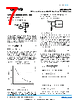
8 / 19 page  Classification | PRIVATE Data Sheet Rev. B, January 2025 | Subject to change without notice 8 of 19 www.qorvo.com © 2025 Qorvo US, Inc. All rights reserved. Qorvo Confidential & Proprietary Information ACT4533A/B Wide Input Sensorless CC/CV Step-Down DC/DC Converter External High Voltage Bias Diode It is recommended that an external High Voltage Bias diode be added when the system has a 5 V fixed input or the power supply generates a 5 V output. This helps improve the efficiency of the regulator. The High Voltage Bias diode can be a low cost one such as IN4148 or BAT54. Figure 4: External High Voltage Bias Diode This diode is also recommended for high duty cycle operation and high output voltage applications. Input Capacitor The input capacitor needs to be carefully selected to maintain sufficiently low ripple at the supply input of the converter. A low ESR capacitor is highly recommended. Since large current flows in and out of this capacitor during switching, its ESR also affects efficiency. The input capacitance needs to be higher than 10 µF. The best choice is the ceramic type, however, low ESR tantalum or electrolytic types may also be used provided that the RMS ripple current rating is higher than 50% of the output current. The input capacitor should be placed close to the IN and G pins of the IC, with the shortest traces possible. In the case of tantalum or electrolytic types, they can be further away if a small parallel 0.1 µF ceramic capacitor is placed right next to the IC. Output Capacitor The output capacitor also needs to have low ESR to keep low output voltage ripple. The output ripple voltage is: ������ = ������ × (������ + × × ) (6) Where IOUTMAX is the maximum output current, KRIPPLE is the ripple factor, RESR is the ESR of the output capacitor, fSW is the switching frequency, L is the inductor value, and COUT is the output capacitance. In the case of ceramic output capacitors, RESR is very small and does not contribute to the ripple. Therefore, a lower capacitance value can be used for ceramic type. In the case of tantalum or electrolytic capacitors, the ripple is dominated by RESR multiplied by the ripple current. In that case, the output capacitor is chosen to have sufficiently low ESR. For ceramic output capacitor, typically choose a capacitance of about 22 µF. For tantalum or electrolytic capacitors, choose a capacitor with less than 50 mΩ ESR. Rectifier Diode Use a Schottky diode as the rectifier to conduct current when the High-Side Power Switch is off. The Schottky diode must have current rating higher than the maximum output current and a reverse voltage rating higher than the maximum input voltage. STABILITY COMPENSATION Figure 5: Stability Compensation : CCOMP2 is needed only for high ESR output capacitor The feedback loop of the IC is stabilized by the components at the COMP pin, as shown in Figure 5. The DC loop gain of the system is determined by the following equation: ������ = 0.808������ ������ ������ ������ (7) The dominant pole P1 is due to CCOMP: ������ = ������ 2������ ������ ������ (8) The second pole P2 is the output pole: ������ = ������ 2������ ������ ������ (9) The first zero Z1 is due to RCOMP and CCOMP: ������ = 1 2������ ������ ������ (10) And finally, the third pole is due to RCOMP and CCOMP2 (if CCOMP2 is used): ������ = 1 2������ ������ ������ (11) The following steps should be used to compensate the IC: |
|
|
リンク URL |
| ALLDATASHEETはお客様のビジネスに役立ちますか? [ DONATE ] |
Alldatasheetは | 広告 | お問い合わせ | プライバシーポリシー | データシートへのリンク | リンク交換 | メーカーリスト All Rights Reserved©Alldatasheet.com |
| Russian : Alldatasheetru.com | Korean : Alldatasheet.co.kr | Spanish : Alldatasheet.es | French : Alldatasheet.fr | Italian : Alldatasheetit.com Portuguese : Alldatasheetpt.com | Polish : Alldatasheet.pl | Vietnamese : Alldatasheet.vn Indian : Alldatasheet.in | Mexican : Alldatasheet.com.mx | British : Alldatasheet.co.uk | New Zealand : Alldatasheet.co.nz |
|
Family Site : ic2ic.com |
icmetro.com |
 Japanese ▼
 English
 Chinese
 German
 Japanese
 Russian
 Korean
 Spanish
 French
 Italian
 Portuguese
 Polish
 Vietnamese
 Indian
 Mexican
 British
 New Zealand