|
データシートサーチシステム |
|
|
データシートサーチシステム |
|
AD4052BCPZ-R2 データシート(PDF) 6 Page - Analog Devices |
|
|
|||||||||||||||||||||||||||||
AD4052BCPZ-R2 データシート(HTML) 6 Page - Analog Devices |
|
|
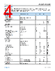
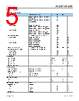
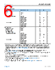
6 / 66 page  Data Sheet AD4052/AD4058 SPECIFICATIONS analog.com Rev. B | 6 of 66 Table 1. Specifications (Continued) Parameter Test Conditions/Comments Min Typ Max Unit VDD 990 nA VIO VIO = 1.8 V 50 nA VIO = 3.3 V 260 nA VDD Active Supply Current 9 Sample Mode and Averaging Mode fS = 10 kSPS 4 μA fS = 500 kSPS (AD4058) 0.2 0.27 mA fS = 1 MSPS (AD4052) 0.4 mA fS = 1.5 MSPS (AD4052) 0.6 0.75 mA fS = 2 MSPS (AD4052) 0.8 1 mA Autonomous Modes fS = 10 kSPS 1.12 μA fS = 300 kSPS (AD4058) 34 67 μA fS = 1 MSPS (AD4052) 112 μA fS = 2 MSPS (AD4052) 224 300 μA POWER DISSIPATION VDD = VIO = 3.3 V Sleep Mode Power Dissipation fS = 0 SPS 430 nW Standby Power Dissipation fS = 0 SPS 4.1 μW VDD Energy per Conversion 1.35 nJ VDD Active Power Dissipation9 Sample Mode and Averaging Mode fS = 10 kSPS 13.6 μW fS = 500 kSPS (AD4058) 0.68 0.89 mW fS = 1 MSPS (AD4052) 1.35 mW fS = 1.5 MSPS (AD4052) 2 2.5 mW fS = 2 MSPS (AD4052) 2.7 3.3 mW Autonomous Modes fS = 10 kSPS 3.7 μW fS = 300 kSPS (AD4058) 112 220 μW fS = 1 MSPS (AD4052) 370 μW fS = 2 MSPS (AD4052) 740 990 μW 1 Sampling rate specifies the maximum sample rate capabilities of the AD4052/AD4058 ADCs. Output data rate is the number of ADC samples that can be transmitted over the serial interface per second and is a function of the serial interface timing specifications. In sample mode and averaging mode, the serial interface bottlenecks the AD4052 output data rate to <2 MSPS. In burst averaging mode and autonomous modes, the output data rate requirements are reduced, and the AD4052 ADC core can operate at the full 2 MSPS. See the Calculating Serial Interface Output Data Rate section for guidelines for estimating AD4052/AD4058 SPI output data rate for each operating mode. 2 VIN+ and VIN− represent the voltages on the IN+ and IN− pins, respectively. The AD4052/AD4058 sample and convert the difference between VIN+ and VIN−. 3 See the Wide Input Common-Mode Range section for a detailed description of the AD4052/AD4058 common-mode input voltage range. 4 In the track phase, the total input capacitance is the sum of CIN and the pin capacitance. In the hold phase, CIN is disconnected from the inputs, and the input capacitance is only the pin capacitance. See Figure 38. 5 The minimum and maximum DNL specifications are guaranteed by design. 6 TUE is defined as the largest deviation from the ideal DC transfer function over the full input range for any individual device. TUE includes the combined effects of zero-error, gain error, and INL error for each device. 7 Autonomous mode TUE applies to the comparator operation. See the Comparator Operation and the Autonomous Modes sections. 8 The averaging REF input current scales linearly with fS (see Figure 21). 9 VDD supply current and power dissipation scale linearly with sample rate (see the VDD Power Dissipation section, Figure 24, and Figure 27). |
|
リンク URL |
| ALLDATASHEETはお客様のビジネスに役立ちますか? [ DONATE ] |
Alldatasheetは | 広告 | お問い合わせ | プライバシーポリシー | データシートへのリンク | リンク交換 | メーカーリスト All Rights Reserved©Alldatasheet.com |
| Russian : Alldatasheetru.com | Korean : Alldatasheet.co.kr | Spanish : Alldatasheet.es | French : Alldatasheet.fr | Italian : Alldatasheetit.com Portuguese : Alldatasheetpt.com | Polish : Alldatasheet.pl | Vietnamese : Alldatasheet.vn Indian : Alldatasheet.in | Mexican : Alldatasheet.com.mx | British : Alldatasheet.co.uk | New Zealand : Alldatasheet.co.nz |
|
Family Site : ic2ic.com |
icmetro.com |
 Japanese ▼
 English
 Chinese
 German
 Japanese
 Russian
 Korean
 Spanish
 French
 Italian
 Portuguese
 Polish
 Vietnamese
 Indian
 Mexican
 British
 New Zealand